No.
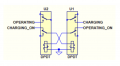
"Charging_on" and "Operating_on" are the respective control signals to the relay coils.
The transistor collectors go to your plus supply voltage.
"Charging" and "Operating" go to the respective Devices' charging and operating circuits.
There are no "Off" control signals as you show, which makes your schematic confusing.
You can call them 'In" or "Out" if that helps your understanding.
Yes but only in part. If the 6 DPDT relay contacts are only dealing with switching signals and not power in/out, then what does the connection going to each of the devices from the relays do, e.g. ‘Device_1’? How is that signal now used to get the device to ‘operate’ or be ‘charged’? Does that ‘Device-1’ signal now have to go to another set of relays to allow the device to either provide power (operate) or receive power (charge)?
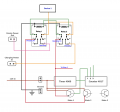
Quite a few comments about the actual drawing, in addition to the point that the relay interlocking is not required.
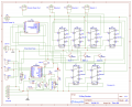
Placing the three transistors at the very bottom makes it more complex than locating the transistors above the two integrated circuits. And none of the required components to make the CD4060 operate are shown. While relay terminal numbers are provided, the IC pin numbers are missing. That makes assembly, or even simulation, difficult.
The 12 volt source positive is shown, a fair guess is that "ground" is the return, while mostly it is not, and never on my designs.
Device in and device out should rather be "device operate supply" and "Device charge supply", to be accurate.
Yes but only in part. If the 6 DPDT relay contacts are only dealing with switching signals and not power in/out, then what does the connection going to each of the devices from the relays do, e.g. ‘Device_1’? How is that signal now used to get the device to ‘operate’ or be ‘charged’? Does that ‘Device-1’ signal now have to go to another set of relays to allow the device to either provide power (operate) or receive power (charge)?
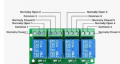
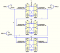
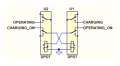
Where are you getting 6 DPDT relays? The device has 4 SPDT relays per the picture: with normally closed contacts on the right and normally open to the left.
Not better, just simpler.
It would appear that the SPDT approach requires logic gates/diodes from the counter to energize the relays in proper sequence (have you looked at that).
The cross-coupled relays don't, as you can see in post #62.
So it's a trade-off between SPST relays with added logic, or DPDT relays requiring none.
Actually, no. And - fun fact - crutschow is incorrect about his own post. See #46 and #49.
As you pointed out in #46, my 6 x SPST solution does *not* require steering diodes to decode the states correctly. One disadvantage of 6 x SPST, that is corrected with 6 x DPDT, is the possibility of cross-conduction between the two power sources. This would be on the order of milliseconds, and the TS has stated that this "probably" is not a problem, but the second set of contacts is used to ensure that this can not happen. A minor advantage of 6 x SPST over 6 x DPDT is cost.
Actually, no. And - fun fact - you are incorrect about your own post. See #46 and #49.
As you pointed out, my 6 x SPST solution does *****not***** require steering diodes to decode the states correctly. One disadvantage to 6 x SPST, that is corrected with 3 x DPDT, is the possibility of cross-conduction between the two power sources. This would be on the order of milliseconds, and the TS has stated that this "probably" is not a problem. The other disadvantage is cost. 6 x SPST probably costs more than 3 x DPDT.
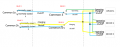
My idea to cover all the conditions of the board are as follows (off, on, and charging), for the three devices. This is a rough out diagram. I have not yet added any Transistors, Diodes etc. to get the job done. That was my next step.
The CD4017 outputs are named "0" through "9", so the three active outputs you use are 0, 1, and 2.
Also, there needs to be a connection between the "3" output and the Reset input. This is what forces the cycle to repeat after only three clock pulses. On the 4th clock pulse, the "3" output goes high, which presents high signal the the Reset input, and the counter immediately goes to the "0" state, your first used output. The counter is in the "3" state for less than a microsecond; this does not affect the time duration of the "0" state.
My idea to cover all the conditions of the board are as follows (off, on, and charging), for the three devices. This is a rough out diagram. I have not yet added any Transistors, Diodes etc. to get the job done. That was my next step.
Your drawing shows the Charging states for all three devices connected together, so all devices are charging at the same time. Same for the Operating state. This is incorrect. Only one device is charging at any point in time.
Your drawing shows the Charging states for all three devices connected together, so all devices are charging at the same time. Same for the Operating state. This is incorrect. Only one device is charging at any point in time.
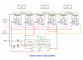
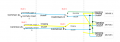
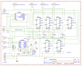
Sorry about the drawing (that was not my latest one). Here is the latest one:
This is still a work in progress in an attempt to use 4 relays for control and yes, it appears to have them in parallel. But look closely at the combination of relay outputs. And yes at the moment it appears they are all in parallel.
Quite a few comments about the actual drawing, in addition to the point that the relay interlocking is not required.
Placing the three transistors at the very bottom makes it more complex than locating the transistors above the two integrated circuits. And none of the required components to make the CD4060 operate are shown. While relay terminal numbers are provided, the IC pin numbers are missing. That makes assembly, or even simulation, difficult.
The 12 volt source positive is shown, a fair guess is that "ground" is the return, while mostly it is not, and never on my designs.
Device in and device out should rather be "device operate supply" and "Device charge supply", to be accurate.
Quite a few comments about the actual drawing, in addition to the point that the relay interlocking is not required.
Placing the three transistors at the very bottom makes it more complex than locating the transistors above the two integrated circuits. And none of the required components to make the CD4060 operate are shown. While relay terminal numbers are provided, the IC pin numbers are missing. That makes assembly, or even simulation, difficult.
The 12 volt source positive is shown, a fair guess is that "ground" is the return, while mostly it is not, and never on my designs.
Device in and device out should rather be "device operate supply" and "Device charge supply", to be accurate.
Referring to the circuit in post #55 - Still two relays per device, so while the logic structure is different, I don't see any clear advantage over the other solutions.
IMHO, I would tie the relay coils to Vdd and switch them to GND, eliminating two transistors per device.
Also, starting with a single clock source, it would be interesting to see the logic that drives the relays.
I did *****not**** point that out.
If 6 SPST relays do not require steering diodes (or other added logic), please show how that is possible for the three states.
How does that eliminate transistors?
My circuit only requires three.
That also inverts the logic.
For my circuit it is simply the output of the CD4017 counter with a reset at count 4.
I did *****not**** point that out.
If 6 SPST relays do not require steering diodes (or other added logic), please show how that is possible for the three states.
After a little further though, I realize you don't need steering diodes if using 6 relays.
Each state has two relays energized just once per cycle, so just connect the relay driver (3 needed, could be NPN emitter followers) from each of the three counter outputs to the two relays energized for each state.
Here is the schematic. I'm not sure if I need any resistors in the feeds from the counter U1 to the bases of Q1-3. I'm also assuming that U1 starts its cycle at output 0 and not 1.
Getting everyone to agree if this will work could be a problem it seems
I have added the reference design as well.

 Facebook
 Google
 GitHub
 Linkedin