3.3V GPIO to 5V Amplification

Thread Starter

Luckyguide

Joined Feb 28, 2025
35
Dear all,

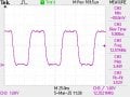
I need to convert the output of my 3.3V GPIO pin to a 5V signal. I am connecting the 5V output directly to the input of a CCD sensor. In total I have 6 timing signals that have to be sent out to from the FPGA to the sensor and all of them have to be converted from 3.3V to 5V. The frequency of these signal are very high as 1 signal has a 50% duty cycle at 12.5MHz. Another signal has a frequency of 12.5MHz with a 25% duty cycle. These are the fastest signals that have to be converted. In general i would like to keep the originality of the signal as much as possible with as little noise as possible. I was thinking of MOSFETS with dedicated MOSFET drivers(because the current from my FPGA is only 8mA) or CMOS to TTL converters. Does anyone have any suggestions on some good components or perhaps other ways to achieve this voltage amplification?

I have attached the signal below for better clarity, if I didn't mention something feel free to ask.
 

Attachments

ronsimpson

Joined Oct 7, 2019
4,649
The frequency of these signal are very high as 1 signal has a 50% duty cycle at 12.5MHz. Another signal has a frequency of 12.5MHz with a 25% duty cycle.
There are many "Mick Mouse" ways of doing lever translation. They might not work at 12mhz 25% duty cycle. Also, they will not work well if there is noise or long distances between parts.
The 5V IC may work just fine with a 3V signal. Look at the data sheet.
At these speeds use a level translator IC!
 

MrChips

Joined Oct 2, 2009
34,629
At higher frequencies, what is going to make or break this is the RC time constant in the signal path.
Start with R = 10 kΩ and gradually decrease the resistance to 1kΩ while vetting it with an oscilloscope.
 

0ri0n

Joined Jan 7, 2025
161
Does anyone have any suggestions on some good components or perhaps other ways to achieve this voltage amplification?
Use logic gates from the HCT family. These are compatible with 3.3V input logic levels when supplied with 5V. For even higher frequencies you can switch to the ACT family.
 

Thread Starter

Luckyguide

Joined Feb 28, 2025
35
Thanks for the responses,

I have decided that I will try several options by testing a: dual-part, logic gates, MOSFETS, simple level shifter, and a single bit dual supply bus transceiver. I will give an update on what the best possible solution is when I find out!
 

MrChips

Joined Oct 2, 2009
34,629
Thanks for the responses,

I have decided that I will try several options by testing a: dual-part, logic gates, MOSFETS, simple level shifter, and a single bit dual supply bus transceiver. I will give an update on what the best possible solution is when I find out!
You forgot the obvious one, a straight connection with no additional components.
 

Thread Starter

Luckyguide

Joined Feb 28, 2025
35
I didn't, that was what I meant by simple level shifter.

It worked really well though with high frequency signals. It was easily able to keep up with the 25MHz signal but the output signal was only 4.1 Volts which was not enough. Further increase of the 5V power supply would destroy the GPIO pin of my development board when the diode would be in forward bias so the simple level shifter is limited by voltage output but can go well with high frequencies. Perhaps you know of a way to increase voltage output to 5V while keeping current and voltage below 4V on the GPIO when the diode is in forward bias?
 

MrChips

Joined Oct 2, 2009
34,629
I didn't, that was what I meant by simple level shifter.

It worked really well though with high frequency signals. It was easily able to keep up with the 25MHz signal but the output signal was only 4.1 Volts which was not enough. Further increase of the 5V power supply would destroy the GPIO pin of my development board when the diode would be in forward bias so the simple level shifter is limited by voltage output but can go well with high frequencies. Perhaps you know of a way to increase voltage output to 5V while keeping current and voltage below 4V on the GPIO when the diode is in forward bias?
Why do you want to increase the voltage if 4 V works fine?
 

Thread Starter

Luckyguide

Joined Feb 28, 2025
35
Because the datasheet for my CCD sensor states that the minimal values need to be 4.5V and 5V ideally. Perhaps I miscommunicated, I am first trying to achieve the right power for my signal, after which I will integrate it into my circuit.
 

MrChips

Joined Oct 2, 2009
34,629
Because the datasheet for my CCD sensor states that the minimal values need to be 4.5V and 5V ideally. Perhaps I miscommunicated, I am first trying to achieve the right power for my signal, after which I will integrate it into my circuit.
Can you post the datasheet of the CCD sensor?
 

AnalogKid

Joined Aug 1, 2013
12,050
Where were you when I needed that! I used a CMOS buffer that could trigger at 3V.
That's what I was going to recommend. Something in the 74ACT line would be perfect for this. If you invert the six output signal polarities inside the FPGA, then one 74ACT04 can buffer and drive all six with one very common component plus one power supply decoupling cap. Good for at least 100 MHz.

Page 4:
https://www.onsemi.com/download/data-sheet/pdf/74act04-d.pdf

ak
 
Last edited:

AnalogKid

Joined Aug 1, 2013
12,050
Here is the simplest 3.3 V to 5 V level shifter. R1 can be 1k to 10kΩ.
For lower values of R1, the diode's Vf plus the GPIO low-state voltage might be too high for the CCD part to see a logic zero.

Also, the 3.3 V system might not be too happy having 4.4 v impressed upon it. If the output is a GPIO pin that has input transient protection diodes all the time, that diode's Vf plus D1 will be less than 1.7 V.

ak
 
Last edited:
Top