Would be Thankful for a check over of my PCB Design before Producing.

Thread Starter

TonyAm

Joined Oct 12, 2022
83
Hello,

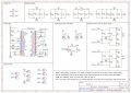
I have a pcb made with easyEDA which uses an Arduino Nano v3 and makes use of a audio synth library called Mozzi (pwm output).
Would be great and sincerely appreciated if anyone could check over for errors before I go and order the pcb's.

MIDI input with opto coupler, and also circuitry for MIDI output, however not used at the same time, switched with jumpers. There is a PWM output from D3 of Nano to audio circuit (volume pot and passive LPF), there is also an optional PWM output from D9 (not shown in schem) but switched on with jumper. *D3 is also used as the TX of MIDI when not being used for PWM, and there is a 6 pin jumper (JP1) for selecting either D3 or Nano's built in TX pin.

Sincere Thanks for any help or advice.
TonyAme
 
Last edited:

samunal

Joined Jul 3, 2024
26
If you are designing the PCB and schematics first time here are some suggestions: The design made by you maybe a correct one, but to interpret the connections a senior design may find some difficulties. For better and reproduceable schematics design:
1) Don't route wires over all of schematics, instead use net lable or net port given in Easyeda
2) Make proper sections of the scheamtics including power, input, output, control, microcontroller etc.
3) GND and VCC should be clearly visible and heads toward their reference positions.
here is the one you can refer to, I made 100w amplifier design. By the way comments in a design scheamtics helps a lot which are already there in your design. I would recommend to use JLCPCB if you are using EasyEDA because of platform intergration.
 

Attachments

Thread Starter

TonyAm

Joined Oct 12, 2022
83
I see what you're saying. Will study your schematic. I see how you grouped things in a logical/ordered way.
Yes, been using jlcpcb, so far I have been very lucky, but things can get confusing very quickly. Sincere thanks for that.

TonyAm
 

Jon Chandler

Joined Jun 12, 2008
1,560
One thing to note – there are a lot of personal quicks in laying out schematics. One person's nice schematic will drive other people nuts. For example, @samunal said you should use more net labels instead of connections stretching across the page, while in another post, someone criticized your "netlist schematic." You can't please everybody – the goal is a clear, unambiguous schematic.

One place I definitely recommend a netlist approach is with power and ground connections. For example, instead of running a ground connection across the page, use ground symbols for connections that are close together, but use ground symbols wherever it makes sense.

Having mounting holes on the schematic is a good touch; otherwise EasyEDA deletes manually placed holes on the circuit board every time you update.
 

Thread Starter

TonyAm

Joined Oct 12, 2022
83
One place I definitely recommend a netlist approach is with power and ground connections. For example, instead of running a ground connection across the page, use ground symbols for connections that are close together, but use ground symbols wherever it makes sense.
Yes, I see there is some middle ground, not too much rats nest. My schems have been getting a little closer to confusing, learning some of Samunal's method helps. There's a balance, like Rush's "Hemispheres" album had told. (I'm a bass player).
Sincere thanks,
TonyAm
 

samunal

Joined Jul 3, 2024
26
Circuit having more than 50 components, routing nets all over the schema is not recommended at all. But on the other hand use of lables increase the readability.
 

Jon Chandler

Joined Jun 12, 2008
1,560
Circuit having more than 50 components, routing nets all over the schema is not recommended at all. But on the other hand use of lables increase the readability.
Different strokes for different folks. Others think differently. There is no one right way to draw a schematic or to design a circuit.
 
If you are designing the PCB and schematics first time here are some suggestions: The design made by you maybe a correct one, but to interpret the connections a senior design may find some difficulties. For better and reproduceable schematics design:
1) Don't route wires over all of schematics, instead use net lable or net port given in Easyeda
2) Make proper sections of the scheamtics including power, input, output, control, microcontroller etc.
3) GND and VCC should be clearly visible and heads toward their reference positions.
here is the one you can refer to, I made 100w amplifier design. By the way comments in a design scheamtics helps a lot which are already there in your design. I would recommend to use JLCPCB if you are using EasyEDA because of platform intergration.
but I find your schematic is more confused than his

You should clariffy the PMOS to make it work. but a simple rectifier diode is much easier for your design!
 

samunal

Joined Jul 3, 2024
26
but I find your schematic is more confused than his

You should clariffy the PMOS to make it work. but a simple rectifier diode is much easier for your design!
Each section is clearly labelled if you still find it confusing then I think basics can be revised once again.
 
Top