Why are (much) wider PCB traces being used for SHF LDMOS fet Gate and Drain connections?

Thread Starter

rschulting

Joined Jul 26, 2023
12
Hi All,

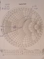
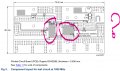
I succesfully designed and build RF driver amplifiers (up to 5W DATV) for VHF and UHF. I now started to do the same for SHF (and higher, 23cm and 13cm) so I looked around for examples and found many of them using wide PCB pads at the gate and drain, sometimes different sizes stacked after each other. Thus far I designed the impedance matching using the conjugate of the LDMOS fets published impedance data. Why is the approach different on higher frequenties I wonder. I know about stepped impedance transformers, how they operate but when do you start using them instead of regular striplines (CPW)? I'm attaching a picture showing the area of interest.

Thx for your kind help!
Richard (PA1RAM)
 

Attachments

ZCochran98

Joined Jul 24, 2018
351
This is still a form of conjugate matching, so in that regard nothing has changed, but at higher frequencies (~1 GHz and higher, from my experience) discrete components can have bad parasitic properties or are large enough to be appreciable fractions of wavelengths, so we start relying on microstrip lines to do the transformations/matches (the lines here are mostly microstrip; the ground planes on top are close enough that there may be some weird hybrid microstrip/grounded coplanar waveguide thing going on). What you're seeing there is a very low impedance right at the gate and drain, to which the bias lines connect. The fat lines coming off of the gate and drain are there to start the transformation back up to 50, but because the impedances are so far from 50 the line has to start out at a pretty low impedance. I've done some designs with low-impedance lines on the transistor that are as wide as or bigger than the transistor itself (admittedly not always a good idea).

Additionally, another reason you'd use microstrip over CPW is for PCB manufacturing reasons (until you start getting into RF ICs), as it's a LOT easier to manufacture a microstrip line rather than a CPW line (or its cousin, the grounded CPW, which is CPW with a back ground plane), because of the line spacing required (4 mil is usually the spacing limitation I've seen), plus fewer overall required GND vias for your ground plane via fencing. Combine this with reducing the amount of soldering and component assembly and you've got another reason why we go to microstrip line-based conjugate matching.

Hope that answers your question!
 

Thread Starter

rschulting

Joined Jul 26, 2023
12
Thank you for your kind reply and explanation which direction I fully understand. I did some calculations on this PCB and others as well and the inductance of these striplines are no where near the conjugate matching. This puzzles me which is why I thought to ask the question here. Suppose I want to design this myself (and no I don't have ADS to help me out) where do I start? Is this line supposed to have the impedance from e.g. the Gate. According to the datasheet at 1800MHz the impedance is (1.6 -j 5.5)Ω. Do I then dimension the trace width to match 1.6Ω impedance wise and then make it long enough to form the required inductance (with capacitors) to build the conjugate? I know it's all about having the lowest reflection looking into this pad from the 50Ω signal line. I'm just trying to understand the dimensions on these PCB's.

By the way, most of these PCB's have a full copper backplane
 

ZCochran98

Joined Jul 24, 2018
351
Do I then dimension the trace width to match 1.6Ω impedance wise and then make it long enough to form the required inductance (with capacitors) to build the conjugate?
I missed that part of the question. More or less, yes, that's the idea. You have to choose an appropriate characteristic impedance to do so. Smith charts are a fantastic tool for doing this kind of thing, if you are familiar with them (thus my question).

Edit: for the simplest possible match, you'd define your line to have an impedance of closer to 9 Ohms and then make it sufficiently long (9 Ohms is the geometric mean of 50 and 1.6).
 
Last edited:

Thread Starter

rschulting

Joined Jul 26, 2023
12
Yes I am familiar with smith charts, been using it as well for the previous designs at 2m and 70cm, worked like a charm. So I had to lookup geometric mean, get it now, but why the geometric mean? Anyway wouldn't this create a mismatch at the Gate? Will do some examples in the smith chart tomorrow to see the direction into which this is going. Thanks again!
 

ZCochran98

Joined Jul 24, 2018
351
Once you've done a little practice with the smith chart I can explain the transmission line process in further detail.

In regards to why the geometric mean: when you use transmission lines on the Smith chart, they trace out circular paths, starting at the load impedance and circling around the characteristic impedance of the transmission line, moving in arcs twice the angular length of the line itself (so a 90-degree line forms a 180-degree arc). If you have two (real for now) impedances you want to transform between, you have to choose a center point between them. This center point happens to be the geometric mean between the impedances (because the Smith chart actually is a plot of reflection coefficients, and it requires a conversion between impedance and reflections). So, as an example. a 50-to-100-ohm transformer would be a line with a characteristic impedance of 71 Ohms (and 90 degrees in electrical length).
 

Thread Starter

rschulting

Joined Jul 26, 2023
12
O.k. I'm officially lost in your last explanation. While I do use the Smith Chart, I feel I do not really understand it as I can't follow your last reply. When I studied the chart earlier this year my focus was mainly on impedance matching and while I was able to apply this knowledge on some of my designs I guess I'm still missing some important basic facts to really understand what I'm doing. So this means I will have to go back to the Smith Chart theory first before I can follow up with you and really understand your explanations. This will be my focus in the upcoming weeks.
 

ZCochran98

Joined Jul 24, 2018
351
O.k. I'm officially lost in your last explanation. While I do use the Smith Chart, I feel I do not really understand it as I can't follow your last reply. When I studied the chart earlier this year my focus was mainly on impedance matching and while I was able to apply this knowledge on some of my designs I guess I'm still missing some important basic facts to really understand what I'm doing. So this means I will have to go back to the Smith Chart theory first before I can follow up with you and really understand your explanations. This will be my focus in the upcoming weeks.
Alrighty. Good luck! The Smith chart is a bit..."esoteric" at first. It's also possible (likely) that my explanation (especially without diagrams) was excessively confusing and not well-worded.
 

Thread Starter

rschulting

Joined Jul 26, 2023
12
Hi Z..., my first name is Richard, can I have yours?

Anyway I've been reviewing some training on Youtube I used before (https://www.youtube.com/playlist?list=PLLNp7XoiSLQaZDb07mTKO8L-e0Mhhibz1) and I guess the part you were talking about is rotating the input impedance from the FET towards the source until it crosses the 50Ohm circle (or is it another circle?) and measure the wavelength used for this rotation.

The impedance for the frequency I'm interested in is given as Mag=0,42 with Angle=-156,94 (this is the S11 @ 1240MHz), in cartesian notation this becomes Zin=(21,126 -j8,44)Ω. Obviously this is within a 50Ω system so normalized this becomes (0,42 -j0,17)Ω. I can use this as the starting point within the Smith Chart, however you advised me to use the geometric mean as the line impedance which in this case equals SRT(21,126 x 50)=32,5 in cartesian that would be 0,65.

My issue now is that I don't know where to use this value. You mentioned "when you use transmission lines on the Smith chart, they trace out circular paths, starting at the load impedance and circling around the characteristic impedance of the transmission line." I don't know (yet) how to interpret this, the center of my Smith Chart is still 50 Ohms (normalized to 1) so certainly not equal to the value of the chosen transmission line impedance (0,65).

I'm missing something important here, I hope you can point me in the right direction? I attached a chart I was working on, perhaps it illustrates my issue better...
 

Attachments

ZCochran98

Joined Jul 24, 2018
351
Hi Z..., my first name is Richard, can I have yours?

Anyway I've been reviewing some training on Youtube I used before (https://www.youtube.com/playlist?list=PLLNp7XoiSLQaZDb07mTKO8L-e0Mhhibz1) and I guess the part you were talking about is rotating the input impedance from the FET towards the source until it crosses the 50Ohm circle (or is it another circle?) and measure the wavelength used for this rotation.

The impedance for the frequency I'm interested in is given as Mag=0,42 with Angle=-156,94 (this is the S11 @ 1240MHz), in cartesian notation this becomes Zin=(21,126 -j8,44)Ω. Obviously this is within a 50Ω system so normalized this becomes (0,42 -j0,17)Ω. I can use this as the starting point within the Smith Chart, however you advised me to use the geometric mean as the line impedance which in this case equals SRT(21,126 x 50)=32,5 in cartesian that would be 0,65.

My issue now is that I don't know where to use this value. You mentioned "when you use transmission lines on the Smith chart, they trace out circular paths, starting at the load impedance and circling around the characteristic impedance of the transmission line." I don't know (yet) how to interpret this, the center of my Smith Chart is still 50 Ohms (normalized to 1) so certainly not equal to the value of the chosen transmission line impedance (0,65).

I'm missing something important here, I hope you can point me in the right direction? I attached a chart I was working on, perhaps it illustrates my issue better...
The "Z" is for Zac.

You're on the right track, it looks like. I didn't explain it terribly well, but the center of said circle would be placed at \(0.65\angle 180^\circ\), so at the 0.65 mark on the chart straight to the left of center. Then, you place your compass at that point and draw an arc connecting your load impedance (Zin) to your source impedance (50), as I have in my attached sketch (I have a math error in my drawing because I used the magnitude of the impedance rather than just the real part, so I calculated 33.7 \(\Omega\) rather than 32.5 \(\Omega\) - use 32.5 \(\Omega\) as you calculated!). You then find the angle element by extending out a radius from that center point towards the load and the source impedances, and seeing where they intersect with the external edge of the chart. In this case, the radius towards the load impedance intersects at just past 0.05\(\lambda\) on the "wavelength towards load" circle, and the radius towards the source intersects at exactly 0.25\(\lambda\) on the "wavelength towards generator" circle. The total amount of the outer perimeter it therefore requires is 0.05+0.25 = 0.3 wavelengths, or about 108\(^\circ\).

As a note, if you have a protractor, you can alternatively just measure the angle the circle sweeps out and divide by 2 to get the same angle (this circle goes around 216\(^\circ\), for instance).

This is for a single-line match. There are alternative methods. For instance, you could place down an inductor immediately in front of the load impedance with 1.08 nH (so \(X_L = j8.44\Omega\)), and then have a 90\(^\circ\) line at 32.5 \(\Omega\) immediately between the inductor and the source side, or you could do this with two lines, or any other of an infinite number of combinations.

When you do transmission-line matching, any and all transmission line sections you add have their centers placed on the horizontal axis of the smith chart (so either 0 or 180\(^\circ\)), and continue from the endpoint of the last section of the impedance match. Your transmission line sections are then added from load side to source side (so, if you put your source on the left of your schematic and your load on the right, each subsequent section is added to the left of the prior one, starting at the load). The very first transmission line section, therefore, begins at the load. Furthermore, you place your source impedance mark at its conjugate. In the \(Z_S = 50\,\Omega\) case, that's pretty simple, but if you were matching to a different source impedance instead, then you'd need to remember to put the source mark at the conjugate rather than the original value.
View attachment CCI_000010.png


Hope this helps!

.
.
.

Additional info:

This link has a pretty good explanation as to why the geometric mean. The more generalized (i.e.: non-quarter-wavelength) solution to this problem is more involved, but this is a good start. For this case, because the line isn't going to be much longer than a quarter wavelength, the geometric mean is a good start. In fact, for many situations, it's a good first-approximation, but it'll improvement for other setups. Case-in-point: if your normalized load impedance sat at about, say, \(0.5\angle -90^\circ\) (Edit: this refers to the reflection coefficient, which corresponds to an impedance of 30-j40 \(\Omega\)), then the geometric mean will not give a valid line. Instead, a more generalized form of the impedance calculation can be, if you define your load reflection coefficient as \(\Gamma_L\) and your source reflection coefficient as \(\Gamma_S\) (recalling that \(\Gamma = \frac{Z - Z_0}{Z + Z_0}\) and, vice-versa, \(Z = Z_0 \frac{1 + \Gamma}{1 - \Gamma}\)), then your transmission line characteristic reflection coefficient (and, correspondingly, impedance) is calculated by (if I did my arithmetic right):

\[\Gamma_c = \frac{1}{2}\frac{\left|\Gamma_L\right|^2 - \left|\Gamma_S\right|^2}{\Re\left(\Gamma_L - \Gamma_S\right)}\]
\[Z_c = Z_0\frac{2\Re\left(\Gamma_L - \Gamma_S\right) + \left|\Gamma_L\right|^2 - \left|\Gamma_S\right|^2}{2\Re\left(\Gamma_L - \Gamma_S\right) - \left|\Gamma_L\right|^2 + \left|\Gamma_S\right|^2}\]

If \(\Gamma_{L,S}\) corresponds to load and source impedances with magnitudes \(Z_{L,S}\) and phase angles \(\phi_{L,S}\), respectively, then this comes out to:

\[Z_c = \frac{ Z_0\left(Z_L^2 - Z_S^2\right) + 2Z_LZ_S\left(Z_L\cos\phi_S-Z_S\cos\phi_L\right)}{Z_L^2-Z_S^2 + 2Z_0\left(Z_L\cos\phi_L - Z_S\cos\phi_S\right)}\]

With this equation, the "actual" characteristic impedance should be closer to 31.4 \(\Omega\), with a phase length of 101\(^\circ\) (or \(0.28\lambda\)), which is pretty close to the results we got using the geometric mean.

It should now be noted that you cannot do single-line matching for any arbitrary impedance pair. If your circle somehow ends up taking you outside the Smith chart on its path, then it's not a valid solution (as that's a non-passive structure). For example, the weird case (\(\Gamma_L = 0.5\angle -90^\circ\)) has no solution at all if you try to match it directly to 50 \(\Omega\), and if you tried matching that impedance to 5 \(\Omega\) instead, then the center of the circle would end up lying off the chart. Either one would be possible with two transmission line sections, however. The impedance done in these examples as well would work with two sections quite well as well (50 ohm and 0.032 wavelengths followed by a 32 ohm at quarter wavelength, from load to source).
 

Attachments

Thread Starter

rschulting

Joined Jul 26, 2023
12
Hi Zac, Wow!
This is an excellent answer, more then I expected and one that I can surely use to study this matter further which I will do in the coming days. Thank you very much and I will let you know the results.
 

Thread Starter

rschulting

Joined Jul 26, 2023
12
Hi Zac,

I've been doing some calculations/measurements again trying to come up with this wider PCB trace at the input using our previous data. However I end up with a much smaller width of some 3mm instead of the expected 20mm or so. I did some reverse calculations on the test PCBs from Ampleon and don't really understand how they end up with such a wide PCB trace.

I've taken notes about what I have been doing so I can always relate back if I need to do this again. I'm sharing them as PDF. Can you have a look and perhaps provide some feedback to get me on the correct road again? If you want them in Word format, just let me know.

Thank you very much for your help.

Richard.
 

Attachments

ZCochran98

Joined Jul 24, 2018
351
Skimming over your notes, I see you calculated (through a good bit of reverse-engineering) the line's impedance is 7.2 \(\Omega\). This is actually very close to what I was expecting that line to be. Earlier in the discussion, you stated the device had an input gate impedance of (1.6 -j 5.5)Ω, but then later on you say it is (21.126-j8.44)Ω. Looking through your document, I see where you got that number, based on the screenshot you have in it. It looks like an .s6p file, so I went to Ampleon's website itself, seeing if I could find documentation or, better yet, load-pull data, which should give the ideal source and load match points for either gain or efficiency (depending on the design goal).

I found the Keysight ADS model library from Ampleon's website and the .s6p file you were referencing. To my surprise, after reading it, all that .s6p file contains are just the S-parameters from the package itself! The transistor model data is likely in the .ds file instead, and therefore inaccessible to me without Keysight ADS installed on my personal machine (curse you, $100k software!). So, the impedances you're looking at in your documentation/notes are not the transistor impedance matching impedances, but the actual package impedances. I know this because of the note in the .s6p that states "Exported from HFSS 2015.1.0" on line 2 and, on line 1, "Touchstone file from project Driver_Package_Study1." So, that resolves why your impedance is so different. Let's look at the datasheet instead and see what we can come up with.

Looking at the datasheet, I found the load-pull data I was looking for. At \(V_{DS} = 28\) V and \(I_{Dq} = 180\) mA, it has source and load impedances listed for the device. For the BPL9G0722-20G device, your source impedance is somewhere between (0.6-j1.4) and (1.6-j5.5). By a very crude interpolation at the frequency you're looking at, I'd guestimate a \(Z_s \approx 1 - 3.5j\,\Omega\). Using this with the geometric mean, we get \(\sqrt{1\cdot 50} \approx 7.1\,\Omega\), which is very close to the impedance you calculated that they used in the reference design. Looking at the load side, we can roughly approximate an impedance of 3.5-j1.5 (roughly), so the impedance of the line at the drain side should be very roughly \(\sqrt{3.5\cdot 50}\approx 13\,\Omega\), which would be about 6.5 mm wide (which is close-ish to what it looks like that output line is).

So, in the long run, I think the confusion is coming from where you're getting your input impedance value. Looking at the datasheet, they've already given you (some) impedance points, and a good simulator with the device model should be able to provide a better estimate of the impedances at frequencies, power levels, and bias points the datasheet doesn't provide. The impedances you get from an \(S_{11}\) somewhere seems to only be part of the overall picture.

What I'm not entirely clear on without reading through more of their documentation is whether or not the load and source impedances that Ampleon provides are the conjugate match impedances for the device (i.e.: "present these impedances to the device for optimal matching") or are the actual input/output impedances of the device (i.e.: "these are the impedances you need to actually match to"). I think it's the latter, based on their picture, but I'm not 100% sure.

Now, to address the comments about caps: those shunt caps are there to adjust up and down the admittance circles in the Smith chart. Because the line isn't a quarter wavelength (most likely, anyway), you need additional componants to do the appropriate matching (and a lot of amplifier designs need more than just a single line). Placing the DC blocking cap is a semi-arbitrary process; I like placing it as close to the gate as possible, while others I know push it as far away as possible. But as long as it's there, it doesn't really matter where it is, as long as it blocks DC from other stages or from being shunted straight to ground (like if you had a microstrip shorted stub). As high a capacitance (for RF, anyway), as C6 is, it's just there to have as minimal overall effect on the circuit as possible
 

Thread Starter

rschulting

Joined Jul 26, 2023
12
Again wow... You ARE very quick to respond (not sure what your timezone is, I'm in the Netherlands) and even go deep in the documentation yourselve, I really appreciate your efforts to help me!

I think I understand your feedback but have to digest it a bit more. It looks like you explained how they got to their design. I blindly followed their .s6p file expecting this one to be correct to use. But now I'm not so sure anymore. I've asked Ampleon similar questions in the past but they never respond even though this is a dutch company and I would expect more response to a dutch HAM radio operator. Guess times have changed as previously (in the Philips days) they provided lots of information AND samples to the HAM radio community to experiment. No, these days it's all about commerce, using ADS they are refering to all the time and no I have no budget to invest in a platform like that. it's really freaking expensive! I've started to use LTSpice last year, it helped me a lot to understand some of the designs while playing with all sorts of parameters but the gap between LTSpice and ADS is just too large.

I might end up just copying their PCB but I really hate to do that without understanding how they got to such a design...

Thank you very much Zac. I will study your feedback in detail and make a decission for my follow-up. I've learned a lot from you in just a few weeks, it is much appreciated!
 

ZCochran98

Joined Jul 24, 2018
351
Happy to be of help! Where I'm at is in EST timezone, so quite a few hours behind the Netherlands. I wish you luck! Doing higher frequency RF design without the fancy tools gets very complex quickly, but it can be done. I'd recommend you look up an RF design textbook by Cripps, and another by Pozar. Both are great resources for higher frequencies (though Cripps does a lot with BJT-style transistors), and show techniques that can be done by hand.
Keysight ADS is "The" standard design tool nowadays, with its competitor Cadence AWR (formerly "Microwave Office" before Cadence acquired them). I think Qorvo may have a variation of SPICE/LTSPICE that may be open-source? I'm not sure.
 

Thread Starter

rschulting

Joined Jul 26, 2023
12
Hi Zac,

Actually the Moore's Lobby Podcast (see top right in this forum) is about QSpice, only listened the first minutes, will need to find an hour for the remainder. Thus far I've only used LTSpice and using is perhaps a bit too much though...

Now about my PCB endeavour, I spent the majority of last weekend to find more data of this LDMOS fet. I found a tool DSDUMP exists from PathWave which translates a DS file into a HDF5 file. The tool is part of the PathWave Data Tools and seems to be part of ADS as well and it works with Phyton. So I thought why not install ADS and see if I can make the tool working without an ADS license but that was one road too far as the Phyton environment settings are for the ADS directories and I don't know what else isn't configured as expected for Phyton to run this tool. Bummer...:(

I've now used quite some time figuring out the correct PCB layout, I learned a lot (from you) which I will use for sure another time but this time I think I will copy the PCB details from Ampleon. Maybe the layout will be a little less perfect but it's only 30dBm ánd I have some fellow HAM radio amateurs eagerly waiting for my design as well (we are a local group interested in DATV for which we want to build the amplifiers ourselves). This decission is against my normal thought process though...

About the Load Pull data from the data sheet, what they present is the impedance looking out of the FET into the matching network. So I think "these are the impedances you need to actually match to". I'm attaching a doc about it.

So I don't know if this is the end of this topic, I guess so. Anyway I'd like to thank you one more time, you helped me a lot!

Kind regards,

Richard (PA1RAM)
 

Attachments

Thread Starter

rschulting

Joined Jul 26, 2023
12
Hi Zac, I almost finished this project and like to share the results with you as you have been very helpfull while I was designing this driver amplifier.

This is the schematic diagram:
23cm driver amp diagram.jpg

This is the PCB I designed:
PCB layout.jpg

This is the prototype build:
PCB assembly picture.jpg

This was the input impedance:
input impedance before adjustment.jpg

The same after I tuned it:
input impedance after adjustment.jpg

This is the DATV signal output on my SA, well above the 5W target:
Output on SA.jpg

The second harmonic is at -30dBc (which initially was larger than the 1st...):
2nd harmonic at -30dBc.jpg

It took quite some tuning at both the input as the output circuit. Trying different capacities at different locations. But at the end it is delivering the designed output after all. Still need to build a LPF as the 2nd harmonic is way to strong.

Anyway, just liked to share the results with you, maybe you wanted to know how it ended up. Again thx much for your help!
 

ZCochran98

Joined Jul 24, 2018
351
Very nice (and quite a bit of power)! Tuning is always a pain, especially if you don't have any of the expensive design tools (and even if you do, for that matter). And a very close match there on your smith chart. Happy to have been some kind of help. For that second harmonic, a LPF should be relatively simple to build or acquire (depending on your rolloff spec) - especially given that it's already -32 dBc.
 
Top