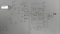
What would be the output of this circuit ?

Thread Starter

niketshah147

Joined Feb 3, 2017
6
circuit.jpg Please ignore the blue ink part.

Kindly let me know what would be the waveform at output?

I am not testing anyone's knowledge here, I just want to discuss this, even I don't know why the waveform at output shows +10 to -10 v, square wave at 2k Hz freq.

View attachment 120080
 

LesJones

Joined Jan 8, 2017
4,544
My calculations (9.1V x 104.99/100 would suggest that the output would be +/- 9.55409 volts. If you are getting +/- 10 volts then it could be component tolerances. The data for the 9.1 volts zener gives 2% tolerance but that would only take the output to +/- 9.745 volts if they were at the top end of their tolerance. Maybe someone else will spot the error in my calculations.

Les.
 

Thread Starter

niketshah147

Joined Feb 3, 2017
6
Hello,

@LesJones , the zener diodes are 9.1 Volts, but in reverse they are about 0.7 Volts.
The output voltage would be (9.1+0.7) X (104.99/100) = 10.29 Volts.

Bertus
Hi,

Thanks for the reply.

I want to understand whole circuit from starting to end. I am failing to convince myself that I am correct. Can you please help to understand this?
 

LesJones

Joined Jan 8, 2017
4,544
When the input 5 volt squre wave is at 0 volts pin 3 of U21A will be at about -1 volt when the 5 volt square wave is at +5 pin 3 of U21 will be at about +2 volts so the output at pin 1 of U21A will swing almost from - 15 volts to + 15 volts R99 will provide some positive feedback improving the switching speed D11 and D13 will clamp the input pin 5 of U21B to +/- (9.1 + 0.7 volts) = +/- 9.8 volts (Note I originally forgot to include the 0.7 volts drop os the zener diode when it was conducting like a normal diode.) The emitter followers from the output of U21B just provide current gain to drive the output load. the gain of the op amp and emitter follower is defined by the ratio of (R109 + R110)/R110 (Normal op amp theory.) So the output voltage is +/- 9.8 volts x 104.99/100 = +/- 10.29 volts

Les
 

Thread Starter

niketshah147

Joined Feb 3, 2017
6
When the input 5 volt squre wave is at 0 volts pin 3 of U21A will be at about -1 volt when the 5 volt square wave is at +5 pin 3 of U21 will be at about +2 volts so the output at pin 1 of U21A will swing almost from - 15 volts to + 15 volts R99 will provide some positive feedback improving the switching speed D11 and D13 will clamp the input pin 5 of U21B to +/- (9.1 + 0.7 volts) = +/- 9.8 volts (Note I originally forgot to include the 0.7 volts drop os the zener diode when it was conducting like a normal diode.) The emitter followers from the output of U21B just provide current gain to drive the output load. the gain of the op amp and emitter follower is defined by the ratio of (R109 + R110)/R110 (Normal op amp theory.) So the output voltage is +/- 9.8 volts x 104.99/100 = +/- 10.29 volts

Les
Thanks a lot Les.
@LesJones @bertus
Can you please tell me what is the role of capacitors in this circuit? How are the helpful here ?
Are these placed to reduce gain during high frequency?
Can you please explain?
 

LesJones

Joined Jan 8, 2017
4,544
C51 & C52 are decoupling capacitors. The ensure that the op amps see a low impedance power supply at higher frequencies. They should be placed as close as possible to the power pins of the IC. C53 is probably to reduce the risk of the op amp oscillating at some high frequency. It will also slow down the transitions of the square wave very slightly.

Les.
 

Thread Starter

niketshah147

Joined Feb 3, 2017
6
C51 & C52 are decoupling capacitors. The ensure that the op amps see a low impedance power supply at higher frequencies. They should be placed as close as possible to the power pins of the IC. C53 is probably to reduce the risk of the op amp oscillating at some high frequency. It will also slow down the transitions of the square wave very slightly.

Les.
Thanks a lot Les. I appreciate the way you are helping me.
I think you have got a good hold of basics of electronics. Can you please suggest me other websites where I can understand the concepts of op-amps and transistor?
 

Thread Starter

niketshah147

Joined Feb 3, 2017
6
When the input 5 volt squre wave is at 0 volts pin 3 of U21A will be at about -1 volt when the 5 volt square wave is at +5 pin 3 of U21 will be at about +2 volts so the output at pin 1 of U21A will swing almost from - 15 volts to + 15 volts R99 will provide some positive feedback improving the switching speed D11 and D13 will clamp the input pin 5 of U21B to +/- (9.1 + 0.7 volts) = +/- 9.8 volts (Note I originally forgot to include the 0.7 volts drop os the zener diode when it was conducting like a normal diode.) The emitter followers from the output of U21B just provide current gain to drive the output load. the gain of the op amp and emitter follower is defined by the ratio of (R109 + R110)/R110 (Normal op amp theory.) So the output voltage is +/- 9.8 volts x 104.99/100 = +/- 10.29 volts

Les
I got confused.

I think opamp U21A is working in saturation condition so it should produce 80% of what we supply at pin 8 & 4. So, in this case where we are applying +15 and -15, we will get +12 and -12.
I am new in this field, so I am applying whatever I am reading and understanding.

Please feel free to give me advice and suggestions.
 

ebeowulf17

Joined Aug 12, 2014
3,307
I got confused.

I think opamp U21A is working in saturation condition so it should produce 80% of what we supply at pin 8 & 4. So, in this case where we are applying +15 and -15, we will get +12 and -12.
I am new in this field, so I am applying whatever I am reading and understanding.

Please feel free to give me advice and suggestions.
I'm not sure where the 80% figure came from, but there isn't any one universal saturation value. You have to look at datasheets to get an idea of the output characteristics of any given op amp. Some are rail-to-rail, meaning their outputs can get amazingly close to the supply voltages, while others can only get within 2V or so of their supply rails.

With a +/-15V supply, the op amp in your schematic can reach at least 13.4 to 13.6V on the positive side, and -13.5 to -14.3V on the negative side, depending on load:

IMG_3914.PNG
 
Top