Facebook
 Google
 GitHub
 Linkedin
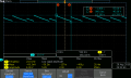
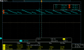
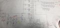
Built this circuit on a PCB, but it is not regulating properly. It is set to regulate at 48V output (at 50V to 100V input). There is about a +/- 10 Volt swing at the output that looks like a ramp. How can this circuit be improved so that there is a 48V output of no more than a 500mV ripple and not a 10V ripple? Please help!
Attachments
-
 108.3 KB Views: 58
")