I just use Eagle (mine is pre-version 8.0), set a 0.1" grid, make a rough outline of the strip board, and do routing in the usual manner, except there are no diagonals. I also use an X to denote either an implied connection that isn't or a cut in a trace. You might want to use top layer for existing copper traces and bottom for connecting wires. I use Kynar 24 awg for connections. Kynar is easy to strip, the insulation is thin, and it doesn't char or shrink back with normal soldering.
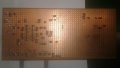
Here's a section of a board that was laid out that way:
The thing I like most is schematic capture. That way, you can be sure all connections are made and there are no wrong ones.
Hi, would you share what brand that board is, please? Or where it came from? I'm trying to make a circuit and that type of board would be ideal for what I want to do. All of the vero/strip boards I've seen just have the copper going from one edge to the other. I like the way that board has a center section going perpendicular to the edges.
I don't remember exactly. I got that version quite awhile ago. Nice, but not through-hole plated. It may be an early version from BusBoard.com (http://busboard.com/products).
More recently, I have gotten virtually identical boards with plated holes from that vendor . Specifically, its SB4 Snappable PC BreadBoard. I have also used the boards from SparkFun. They sure are nice for anything that is not just for a quick experiment.
Note that with the SF board #30 (small), the supply rail holes are staggered relative to the columns for devices. Therefore, I have to make a little hook on resistors and such so they line up to my satisfaction.
The large SF board device does not have that "feature" and everything lines up nicely. It also has connections at the end for the supply rails. A #30 drill (preferably 135° angle, but 118° is OK) works great for cutting tracks and removing a plated pad. For just cutting a track between holes, I use a tiny burr in my Dremel.
Hi, would you share what brand that board is, please? Or where it came from? I'm trying to make a circuit and that type of board would be ideal for what I want to do. All of the vero/strip boards I've seen just have the copper going from one edge to the other. I like the way that board has a center section going perpendicular to the edges.
Hi, would you share what brand that board is, please? Or where it came from? I'm trying to make a circuit and that type of board would be ideal for what I want to do. All of the vero/strip boards I've seen just have the copper going from one edge to the other. I like the way that board has a center section going perpendicular to the edges.
hi,
I would say your layout around the IC is OK.
The rectifier diodes and smoothing caps could be moved closer to the IC group.
Which part of the PCB layout do you think needs reworking.?
I assume the PCB and circuit does actually work.?
E
hi,
I would say your layout around the IC is OK.
The rectifier diodes and smoothing caps could be moved closer to the IC group.
Which part of the PCB layout do you think needs reworking.?
I assume the PCB and circuit does actually work.?
E
 Facebook
 Google
 GitHub
 Linkedin

 65.4 KB Views: 27

")