 Facebook
 Google
 GitHub
 Linkedin
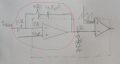
what is this part of circuit ? is it integrator or something else
and what is the expected output in case of Vrf is DC voltage and Isens is sawtooth like signal.
and what is the expected output in case of Vrf is DC voltage and Isens is sawtooth like signal.
Attachments
-
 3.4 MB Views: 40


