Well then if you relax the maximum input frequency value, it will be easier to get the circuit to properly work.There’s no specific design requirements or use case for this. I’m just designing this out of interest and to learn!
Hi Eric, thanks for the help! May I ask why use the voltage dividers for the inputs to U1?Hi Sean,
As this project is a self-teaching project, I would advise a higher performance OPA.
The LT6202 is part of the LTSpice 'F2' OPA listing.
E
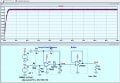
View attachment 372628
Thank you! But why do you need a 0.49 attentuation for vin?Hi Seanm
With resistors R3 & R2 of both 1k, the gain is One for the Inverting Input, BUT Two for the Non Inverting Input.
So the R4 and R5 resistors 100k/96k form a voltage divider for the Input voltage Approx 0.49 attenuation, this also corrects for the forward voltage drop of the Bat54 diode.
E
Since the diode is inside the feedback loop, its forward drop should be divided by ≈1/2 the open-loop gain of the op amp, making it effectively only a few tens of microvolts.Approx 0.49 attenuation, this also corrects for the forward voltage drop of the Bat54 diode.
I have another question, how does this correct the forward voltage drop of the diode?Hi Sean,
With resistors R3 & R2 of both 1k, the gain is One for the Inverting Input, BUT Two for the Non Inverting Input.
So the R4 and R5 resistors 100k/96k form a voltage divider for the Input voltage Approx 0.49 attenuation, this also corrects for the forward voltage drop of the Bat54 diode.
E
Note: Assume a 5Vin signal so: 5Vin (1-0.49) = 2.550v *2gain
Yes, it does now. That part about the diode did confuse me. Thank you for clearing it up.Hi Sean,
That was an incorrect statement on my part, sorry if it caused any confusion.
Does the circuit meet your requirements?
E
I'm missing something: shouldn't it be 5Vin(0.49) instead of 5Vin(1-0.49)?Hi Sean,
With resistors R3 & R2 of both 1k, the gain is One for the Inverting Input, BUT Two for the Non Inverting Input.
So the R4 and R5 resistors 100k/96k form a voltage divider for the Input voltage Approx 0.49 attenuation, this also corrects for the forward voltage drop of the Bat54 diode.
E
Note: Assume a 5Vin signal so: 5Vin (1-0.49) = 2.550v *2gain
| Thread starter | Similar threads | Forum | Replies | Date |
|---|---|---|---|---|
| C | Strange result from I-V curves to characterize photodiodes | Test & Measurement | 10 | |
| E | Multimeter wrong results | Technical Repair | 16 |