Unexpected opamp behavior in a Gaussian-shaped amplifier

Thread Starter

Vilius_Zalenas

Joined Jul 24, 2022
192
Hi,

I am relatively new to analog design but I have fair electronic fundamentals. My task is to build some kind of Gaussian shape amplifier that would transform fixed 1-1.2 us duration voltage spike/square type signal into a Gaussian shape signal with 2-3 us shaping time constant (I will adjust the exact value in the end, shaping time is not the case here.)

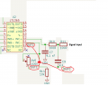
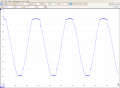
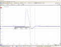
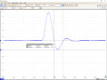
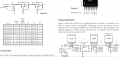
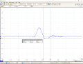
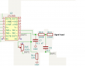
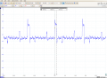
Since this project is related with nuclear particle detection signal processing, I followed a Cremat 200 series Gaussian shaping amplifier (pretty much exact thing I am trying to replicate despite the accuracy, stability etc.) datasheet. They suggest a two stage Sallen-Key filter approach. Seems kind of logical to integrate the signal as long as it takes to turn anything into a sync type function/Gaussian pulse. I am aware that such task may require far more complicated compensation/feedback mechanisms, but again, lets not get lost in the details. I built a circuit just like that: did my RC calculations for approximately 2.5 uS shaping time, picked an appropriate speed, slew rate and bandwidth opamp. I also put a potentiometer to make it gain variable (1-10 times) my opamp supply is +-5V. The input signal has quite some harmonic content in it, because the primary source is a function generator (for testing purposes only.) And in the end, this is just the first Sallen-Key filter stage tested separately, I do not expect to see perfect Gaussian shape pulse, but results are far from that.

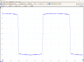
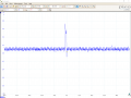
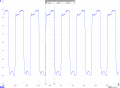
My output signal is a very large amplitude (gain adjustment does not reduce or increase the amplitude) kind of square wave looking signal with next to none integration signs in it. As you can see, the total duration of output signal is 7.3 us which is in the same realm with my shaping time target, but it is still so far from what I am looking for. I have checked my wiring, opamp has solid layout and decoupling. Is there anything I skipped about about analog design dealing with Sallen-Key filters? Any other observations? Thank you in advance.
 

Attachments

MisterBill2

Joined Jan 23, 2018
27,164
Your wiring diagram does not show any feedback connection at all.
The basic concept of an "op-amp" (Operational Amplifier) is that it provides some sort of math operation by means of feedback.
Without a feedback path the amplifier output is not even predictable.
So you need to study and understand the basic functions of operational amplifiers first.
The circuit as shown is a comparator circuit, and a poor one at that.
 

Thread Starter

Vilius_Zalenas

Joined Jul 24, 2022
192
Your wiring diagram does not show any feedback connection at all.
The basic concept of an "op-amp" (Operational Amplifier) is that it provides some sort of math operation by means of feedback.
Without a feedback path the amplifier output is not even predictable.
So you need to study and understand the basic functions of operational amplifiers first.
The circuit as shown is a comparator circuit, and a poor one at that.
There is feedback in my circuit, maybe it looks tricky, but the feedback is really there
 

Attachments

MisterBill2

Joined Jan 23, 2018
27,164
OK, it was not obvious to me because I did not notice the text tag. Still, the gain may have been excessive, that was the symptom based on what the trace looked like. It might be that the feedback was accidentally on pin #9, because the trace does look more like an op-amp used as a comparator. OR maybe there is a DC offset problem.
 

Thread Starter

Vilius_Zalenas

Joined Jul 24, 2022
192
What is C9's value?

And readjust the relative values so R10 and R11 are at least 5kΩ.
I have changed all resistors to 10k and all capacitors to 100 pF to preserve the shaping time near my goal. Situation has changed only slightly. I still get this mad gain of full amplitude. Varying the gain pot either reduces the pulse duration and introduces some kind of more Gaussian looking signal buried deep inside the full amplitude voltage swing (Untitled.png) or extends the signal duration and makes it even more square looking. (Untitled2.png) This time, these voltage swings are in the single digit us range, but still there is constant periodical signal at the output, while my input (Untitled3.png) is set only to 10 Hz during testing. My feedback PCB trace (from the pot to the opamp) is just under 2 inches. I understand its not the best thing for signal integrity etc, but could it really be causing such problems as uncontrollable gain and random periodical signal generation?
 

Attachments

MisterBill2

Joined Jan 23, 2018
27,164
The trace still gives the impression of excess gain taking the amplifier into saturation and cutoff. So it might possibly be that the amplifier supply voltage is inadequate. BUT that is just a guess. What are the supply voltages?
Once again we see only a part of the circuit where the results of the problem are. We get no hint about the rest.
 

Thread Starter

Vilius_Zalenas

Joined Jul 24, 2022
192
The gain pot in you schematic has two two connections to the output so is shorted. but that's apparently not how it's really connected.
So how should be connected?

Below is the LTspice sim of your circuit without the pot.

View attachment 324279
Ok, after extensive experiments I found out that pot was the problem (it was not shorted like you said. It only had one terminal unconnected, but it work from a perspective of a feedback network resistor.)

Just to be clear answering the last question, the opamp`s supply is +- 5V

Problem turned out to be the pot position in the PCB. I cut both tracks of the pot and put a 10k resistor right between the actual opamp package legs. So I have traded my variable gain for the proper signal integration. Can you explain me how does the track length impact the opamp operation so much? Like I mentioned, the pot was located around 2 inches away from the opamp. I am aware of all that EMI stuff, impedances etc. But we are are not talking about an RF signal here. I could understand increased noise, distortion, propagation delays, but it literally made the opamp completely unusable in my case... What are the rules and laws of feedback track laying for the next project? Thanks.
 

sparky 1

Joined Nov 3, 2018
1,218
The nature of Gaussian waves is fascinating. Most have this in a digital function generator but what about analog.
In this paper it describes an OPA656 Gaussian wave shaper designed with the help of simulation software.

A HPF before the 2 sallen-key LPFs are cascaded then followed by a BLR baseline restorer to remove the DC offset.
The schematic provided along with components listed in figure 3 allows the circuit to be simulated in LTspice.
The properties of the square wave before and after filtering in frequency domain or Fast Fourier as experimentation.

Analog Gaussian wave shaping circuit
46091355.pdf (iaea.org)
 
Last edited:

Thread Starter

Vilius_Zalenas

Joined Jul 24, 2022
192
The nature of Gaussian waves is fascinating. Most have this in a digital function generator but what about analog.
In this paper it describes an OPA656 Gaussian wave shaper designed with the help of simulation software.

A HPF before the 2 sallen-key LPFs are cascaded then followed by a BLR baseline restorer to remove the DC offset.
The schematic provided along with components listed in figure 3 allows the circuit to be simulated in LTspice.
The properties of the square wave before and after filtering in frequency domain or Fast Fourier as experimentation.

Analog Gaussian wave shaping circuit
46091355.pdf (iaea.org)
Right, so I solved my problem in general by editing poor PCB layout. Since you mentioned all the shaping circuit topology, maybe you can help me with pole/zero correction?

Now I get near perfect shape Gaussian pulses of wanted duration, but I can not get rid of this pole/zero swing. I read the theory and tried to replicate the P/Z correction circuit from the Cremat application note (Example.png) I tried mix of 100 pF to few of nF capacitors and 10k to 100k pots in various combinations. However, every time it made absolutely no difference to my signal ringing. Theory of P/Z cancelation is widely available and involves quite complex math, but it is often not suitable for direct use in real circuits, as there are too many details to pay attention for it to work. Can you give any observations, common rules or practice-confirmed methods to design a P/Z cancelation circuit, (regarding the P/Z, I have no experience with it)? All the timings and amplitudes are shown in the screenshots. Thank you in advance.
 

Attachments

sparky 1

Joined Nov 3, 2018
1,218
Sometimes you have to repost with a new heading such as
"Pole zero Cremat CR200" non-asymptotic and reflection pulse, really not sure.

I think a post gets buried in the volume, the forum moves so fast we have trouble finding something written 2 days ago.

I use online filter software, the values of inductors and capacitors are close approximation. In less common filters, adapting, is often
trial and error. Usually specific data found in specialized books. Some online filter design pages even give part numbers.
Review and learning curves on all this, that is to further perfect what you already have might take some time and careful experimentation.
Filter Design Tool (ti.com)
 
Last edited:
Top