Understanding Dave Jones' µCurrent device

Thread Starter

cmartinez

Joined Jan 17, 2007
8,722
A few years ago, I bought a µCurrent GOLD device for instrumentation purposes and I'm quite happy with it.

Lately, I've been wanting to replicate the circuit on my own, and after some digging I found this video by Dave Jones himself explaining a stability glitch in the design. One of the comments drew my attention:


@ericksonengineering7011
I see the problem in the schematic. The output stage uses a resistor from the output of the op-amp to the output pin. This R, plus a capacitive load adds a high frequency pole which causes excess phase shift and thus oscillation of the output stage. Move that feedback cap to the op-amp output instead of the board output and increase it a bit, I'd guess 100-1000pF. This was a latent design problem. Spice the circuit and you will see the marginal stability of that stage with a C load. A marginal design is like a blind man walking along the edge of a cliff. If he drifts one way, no problem. If he drifts the other way a tiny bit he falls off. The parameter that is changing slightly is the op-amp phase margin, changing slightly from batch to batch. Fix the design, don't select parts. Hope this helps.
Dave Erickson


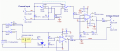
Now, here's Mr Jones' schematic:

1761949604894.png

I have redrawn the above schematic myself, but omitting the TPS3809 chip, and the range selector switch. I have drawn the schematic as it would look like if the range selector switch were set at its most sensitive. That is, in the nano-amps range. For convenience, I have replicated the part numbering as well. The schematic includes the suggested correction at the circuit's output, which is to reconnect C4 directly into the output pin of U4. I have also added C5 for the purpose of being consistent regarding the use of bypass caps.

1761949830714.png

And now for the questions:

  • Have I reconnected C4 correctly? Or is it necessary to also reconnect the right side of R14 the same way?
  • I would like to simulate the circuit in LTSpice, but I cannot find the model for LMV321, which opamp could be used instead?
  • I would like to make a cheaper version of this circuit, by replacing the MX4239 with other zero-drift opamp, if possible. For instance, the NCS333 costs only $0.48 whilst the MAX4239 goes for more than $3.00 buks! ... I know that the NCS333 has entirely different characteristics, but what would happen if said opamp is used instead? ... I would expect that its accuracy (and possibly its response time) would be very affected, but what about stability and repeatability?

If only I had the spice file for the LMV321 I would start exploring the circuit immediately
 

Attachments

xox

Joined Sep 8, 2017
936
Take a look at this repo. Isn't the LMV321 a fairly standard opamp though? You may not even need such a detailed model to get a fairly accurate simulation.
 

Thread Starter

cmartinez

Joined Jan 17, 2007
8,722
Thanks, xox! ... also, I've just found this page containing the complete source files for simulating the device. And I'm finding the place to be gold mine ...

EDIT: The complete project can be downloaded here.
 

Thread Starter

cmartinez

Joined Jan 17, 2007
8,722
Bummer ... I tried to run the sims and I get the following error:

1761960423122.png

I honestly don't understand what it's about ...
 

Thread Starter

cmartinez

Joined Jan 17, 2007
8,722
I've just downloaded an older version of LTSpice (Version 4.23 (Jul 22 2016) and things are running now ... kind of slow and clumsy, though
 

Thread Starter

cmartinez

Joined Jan 17, 2007
8,722
Yeap ... it's working just fine ... I wish I could make it work in the latest 64 version of LTSpice, though ...

1761961562787.png
 

xox

Joined Sep 8, 2017
936
I've just downloaded an older version of LTSpice (Version 4.23 (Jul 22 2016) and things are running now ... kind of slow and clumsy, though
Yep, looks like they're using an older API for the PULSE function.

The old interface was PULSE(V1 V2 TD PW)

V1: initial voltage level (low)
V2: peak voltage level (high)
TD: time delay before the pulse starts
PW: pulse width

Whereas the newer interface is PULSE(V1 V2 TD TR TF PW PER)

TR: rise time (time it takes to go from V1 to V2)
TF: fall time (time it takes to go from V2 back to V1)
PER: period of the pulse

So if you really want to run it on the newest version, you might be able just modify line# 170 of the "uCurrent_nA.asc" file by supplying some "reasonable" values for TR, TF, and PER.
 
Last edited:

Thread Starter

cmartinez

Joined Jan 17, 2007
8,722
Yep, looks like they're using an older API for the PULSE function.

The old interface was PULSE(V1 V2 TD PW)

V1: initial voltage level (low)
V2: peak voltage level (high)
TD: time delay before the pulse starts
PW: pulse width

Whereas the newer interface is PULSE(V1 V2 TD TR TF PW PER)

TR: rise time (time it takes to go from V1 to V2)
TF: fall time (time it takes to go from V2 back to V1)
PER: period of the pulse

So if you really want to run it on the newest version, you might be able just modify line# 170 of the "uCurrent_nA.asc" file by supplying some "reasonable" values for TR, TF, and PER.
Thank you so much for your advice, XOX ... I tweaked the parameters of I1, and voilà! ... it is now working with the latest version of LTSpice at 64 bits. And much faster, of course ... it's just that at first I couldn't understand the software's error message ... now I have a better grasp


1761977214785.png
 

Ian0

Joined Aug 7, 2020
13,097
Connecting the feedback loop to the output of the op-amp instead of after R8 will keep it stable. As connected, the cable capacitance puts a pole inside the feedback loop, which adds 90° of phase shift, which adds to the 90° of phase shift from the op-amps internal compensation and makes a phase shift oscillator. There's no reason for the R8 to be inside the feedback loop. The loss in accuracy due to its acting as a potential divide with a 10M meter input is negligible. You could reduce it to 100Ω if it worries you, or remove it because it will drive a capacitive load of 100pF
C3 and C4 aren't helping either. It looks like they were intended to roll off the frequency response at HF, which they do, but only down to unity, where there will still be enough gain to get it oscillating. The internal compensation capacitor will achieve the same thing without adding extra phase shift. Try removing them.
MAX4239 seems like a poor choice of op-amp. The almost identical, but unity gain stable MAX4238 would seem rather a better choice to me.
I'm also puzzled why there two op-amp stages. The total gain is 40dB and the op-amp is capable of 150dB. The GBW product of 1MHz would give a bandwidth of 10kHz with a gain of 100, which is faster than you're going to be able to read a multimeter. As well as that, an op amp gets more stable as the gain is increased.

LMV321 would seem like a dreadful choice. The MAX4239 was chosen for its low offset voltage, and the LM321 is 4000 times worse. Just how much offset can you cope with? Something like a MCP6071 with 150uV would only result in 15mV at the output.

There's a very nice app note by Analog Devices on driving capacitive loads with op-amps, but I'll be damned if I can find it at the moment. Maybe later.

By the way, in post #9 you seem to have a wire under U1.
 

Thread Starter

cmartinez

Joined Jan 17, 2007
8,722
Thank you so much for your input, Ian. I find it invaluable. Regarding your comment on the LMV321, it is my understanding that it is being used as a voltage divider to create a virtual ground, so maybe its offset voltage is unimportant?

I've redrawn the circuit fixing it at its highest possible gain, that is, set to convert nAmps into mVolts. And for that purpose, I got rid of the selector switches and a couple of resistors and directly connected the participating components. I also got rid of the LED and its driving circuit, and fixed the wire under U1. And following the suggestion I quoted in my first post, I reconnected C4 directly to U4's output, and increased its value to 470pF. The output is now beautifully linear:

1762016855553.png
But when I reconnected the right side of R14 the same way I did with C4, no signal is reported at OUT+ (at the right side of R8, it won't even let me probe it!), although the readings look just fine at U4's output. Maybe R8 is behaving like a floating node in the sim?

1762017332639.png
Anyway, my goal is to make as cheap a version of this circuit as possible. And of course I expect there to be some trade offs. But here are the things that are important to me:

Important:
  • Gain​
  • Stability​
  • Repeatability​

Not important:
  • Offset​
  • Speed​
  • Linearity​

I don't care if the resulting circuit no longer follows a parallel line compared to its input. What's important is that it attains the same output gain in a stable and repeatable way. And of course, using a single opamp instead of two would be preferable.

I have attached the corresponding files for this sim, in case you want to play with it.
 

Attachments

Ian0

Joined Aug 7, 2020
13,097
You have two questions to answer.
1) How good do you want it to be?
2) How good does it need to be?

If you want it to drive a meter not a scope, you can use a single op-amp as you don't need much bandwidth.
I saw a neat circuit on TI's forum using a INA500 to produce a half-supply reference.

I didn't spot the LMV321 down in the corner for some reason and thought you were suggesting it as an alternative to the MAX4239.
 

schmitt trigger

Joined Jul 12, 2010
2,027
@cmartinez;
I made an identical mistake when I designed a constant current load. Many moons ago. I had an opamp driving a transistor, and between the base and the OP’s output a series resistor. Then the feedback capacitor was connected all the way to the base, instead of the OP’s output.

It would oscillate under certain circumstances.
In desperation, I swapped opamp devices until I found one that did not oscillate. A LM358.
I left it like that, not satisfied with the overall performance, but without really understanding what had happened.

Several years later, I realized my error, connected the capacitor correctly to the OP output, and now the circuit wouldn’t oscillate no matter which opamp type I used.
 

Ian0

Joined Aug 7, 2020
13,097
Let's say for a moment, that auto-zero, linearity and temp drift were not important. Can one obtain a x150 gain with a circuit like this one, but using a UMW8631ARTZ or a TP2581-TR instead of the much more expensive MAX4239AUT+T ?


They wouldn't be my first choice because of the relatively high offset voltage, my stock op-amp is the Microchip MCP607x. Offset = 150uV. You will get an offset on the output of 15mV with a gain of 100.
 

Thread Starter

cmartinez

Joined Jan 17, 2007
8,722
I tried importing the spice model of the MCP6071 and, after successfully creating the symbol, I get the following error message​

1762281117132.png

Then I tried to decipher how to correct the syntax for the table being listed in the file, and I'm at a complete loss right now ...
 

Attachments

Ian0

Joined Aug 7, 2020
13,097
I tried importing the spice model of the MCP6071 and, after successfully creating the symbol, I get the following error message​

View attachment 358248

Then I tried to decipher how to correct the syntax for the table being listed in the file, and I'm at a complete loss right now ...
I couldn't get the model to work either. If anyone else can, I'd be interested to know how, but in the meantime, I'll just stick to pen and paper and calculator.
 

Ian0

Joined Aug 7, 2020
13,097
And that's where I get stuck ... I have zilch knowledge of the rules of thumb for calculating the basic performance of an opamp ...
From the equations that everyone knows: non-inverting gain = 1+Ra/Rb, inverting gain = Ra/Rb.
What happens to the offset? It gets multiplied by the gain.
What about noise? voltage noise gets multiplied by the gain, current noise gets multiplied by the source impedance and the gain to give a voltage. Add the two voltages by taking the root of the sum of their squares.
What about bias currents? It's a CMOS op-amp so forget about them unless you want to use stupidly high value resistors.
GBW product: The maximum gain you can possibly get is the GBW product divided by the bandwidth.
Will slew rate be a problem? Not if 2πfVo is less than the quoted value (where Vo = peak output voltage)
And make sure you don't exceed the common mode input voltage.
SPICE will calculate these for you based on a TYPICAL device. What you really want to know is "would it work with a worst-case device".
 
Top