UC3843 smps design frequency problem

Thread Starter

engineer2017

Joined Oct 5, 2020
2
Hi,

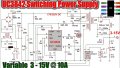
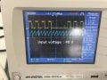
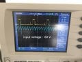
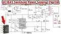
I want to design smps with UC3843 but I have a problem. When the input voltage is changed from 60 to 40 Vdc, frequency is changes. The output voltage does not change.I added smps circuit and switching pulses. Yellow is switching pulse, blue is output of RT/CT pin. What is the problem?
 

Attachments

Papabravo

Joined Feb 24, 2006
21,159
The output voltage is fixed. Did you think that it was a function of the input voltage? Something has to change in order for that to happen. I guess the big red letters must have escaped your notice.
 

Thread Starter

engineer2017

Joined Oct 5, 2020
2
I am so sory. I added the wrong smps circuit. Now, I added used smps circuit in this post. Is the frequency not determined by the triangle waveform?Triangle waveform frequency is stable. You think did it adjust stable output voltage with frequency?
 

Attachments

Dodgydave

Joined Jun 22, 2012
11,285
As the input voltage is lowered, the chip will increase the pwm frequency to give a stronger output, and lower the frequency as the input voltage is increased , thus maintaing a constant output set by the Tl431 Zener, and sensed on pin2 on the chip.
 

ronsimpson

Joined Oct 7, 2019
2,989
What I see is cycle skipping. The frequency of the oscillator is constant.
When I build these the frequency is constant and the duty cycle changes to regulate the output.
What you build outputs maximum duty cycle, but this creates too much voltage so the next cycles are skipped. This is because of your error amplifier has no compensation.
 

Papabravo

Joined Feb 24, 2006
21,159
The output voltage adjustment is via RV1, the pot feeding the TL431. Based on the setting of RV1. If the frequency of the triangle oscillator is fixed, then the controller will alter the duty cycle derived from the triangle oscillator. You should read the datasheet for a complete understanding. Keep in mind there may be multiple feedback loops.

EDIT: There is also slope compensation to prevent sub-harmonic oscillation.
 

ronsimpson

Joined Oct 7, 2019
2,989
There is also slope compensation to prevent sub-harmonic oscillation.
That might be the same as cycle skipping. With out compensation the "error amp" acts as a voltage compare not as a amplifier. As built the TL431 is just looking to see if the voltage is too high or too low. If too low the duty cycle will be at maximum until the voltage is too high, then the duty cycle will be at zero until the voltage sags down.

If you slow down the TL431 it will control the duty cycle, not flip from 50% to 0%.
 

Papabravo

Joined Feb 24, 2006
21,159
That might be the same as cycle skipping. With out compensation the "error amp" acts as a voltage compare not as a amplifier. As built the TL431 is just looking to see if the voltage is too high or too low. If too low the duty cycle will be at maximum until the voltage is too high, then the duty cycle will be at zero until the voltage sags down.

If you slow down the TL431 it will control the duty cycle, not flip from 50% to 0%.
I don't think slope compensation is the same as cycle skipping,
 

Ian0

Joined Aug 7, 2020
9,671
Yes - that's definitely sub-harmonic oscillator or cycle-skipping or whatever you want to call it. It's caused when the duty cycle exceeds 50%, which it should never do on a flyback circuit, otherwise there is continuous conduction and a big increase in diode reverse-recovery losses.
What happens is that the inductor* current fails to reach the threshold set by the error amplifier in the FIRST cycle. There is insufficient off time for the current in the inductor to reduce to zero. The FET switches on again and the current then fairly quickly reaches the threshold. This then repeats every two cycles.
Swap to a UC3845, which has the duty cycle limited to 50%. Slope compensation would be a good idea, but keeping the duty cycle below 50% is more important.
Shouldn't COMP be connected only to the collector of the OPTO and VFB connected to 0V?
Read this on how to compensate your error amplifier. It includes a section on opto-isolator-coupled error amplifiers.

*Although it looks like a transformer on the circuit diagram, it's much more important to think of its operation in terms of an inductor.
 

jtn

Joined Mar 27, 2017
22
The feedback circuit is wrong caused oscillation or pulse skipping mode. U2-4 (opto collector) ties to 5.1V reference through a 1K ohm resistor. U2-3 connects a 1nF to GND. U2-3 connect to PWM 3843 VFM (inverting pin op-amp) through a resistor 15K. Adjust R2 if needed. Add type I compensation network across U1 pin 1 and 3, could try 100nF and 20K at first. Actual compensation network depends on the power section is designed in continuous or discontinuous mode. Good luck
 

Ian0

Joined Aug 7, 2020
9,671
It's a transconductance amplifier, so it is perfectly possible to connect the opto feedback to its output, and by tying FB to ground the error amplifier becomes a constant current load for the opto.
From the TI datasheet:
8.3.4 Error Amplifier With Low Output Resistance The error amplifier output is an open collector in parallel with a current source. With a low output resistance, various impedance networks may be used on the compensation pin input for error amplifier feedback. The error amplifier output, COMP, is frequently used as a control port for secondary-side regulation by using an external secondary-side adjustable voltage regulator, such as a TL431, to send an error signal across the secondary-toprimary isolation boundary through an opto-isolator, in this configuration connect the COMP pin directly to the opto-isolator feedback. On the primary side, the inverting input to the UCx48x error amplifier, VFB, should be connected to GROUND. With VFB tied to GROUND, the error amplifier output, COMP, is forced to its high state and sources current, typically 0.8 mA. The opto-isolator must ove
 
Last edited:
Top