Trying to create board from schematic

Thread Starter

skezza

Joined Jun 17, 2022
9
Afternoon,

I'm new, please be kind :p

I've been soldering for many years and I'm relatively competent at it. I used to modify guitar pedals as a kid and have repaired all kinds of PCB-based electronics, so when this little project came about, I figured how hard could it be :rolleyes:
... Okay, maybe I underestimated the challenge here, so I'm hoping with some advice I might be able to make progress.

There was a company selling PCB kits for a Guitar to Midi converter. I um'd and ar'd for a week too long, they sold the last kit and I was informed they had no more kits coming and had no plans to do another run :(

https://datapoint.uk/midi-boards/guitar-to-midi-converter/

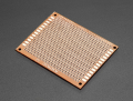
What they did have was the remaining components from one kit, but no PCB and offered them me at a discount. So I took a punt and ordered 20 single layer Perfboards from Aliexpress. https://www.aliexpress.com/item/100...19296979__pc__pcBridgePPC__xxxxxx__1655471141

Following this schematic (inverted as it's single layer), I crack on:
https://datapoint.uk/wp-content/uploads/2021/02/Guitar-to-MIDI-PCB-1.png

So, day 1, and I'm flying through. I'm making a few little tweaks here and there as I didn't really start with any layout or ordering. I was just dropping components on the board. Basically, I went top left across and down.... 5 or so hours later and the whole thing is looking very complicated, but I figured how bad could it be? Today.... I went back and I just couldn't reconcile the board the schematic. I had clearly over-complicated it by my lack of planning. I guess either I need to follow it faithfully or create schematic altogether.. After an hour of trying, I realized (as an experienced software engineer) that if I'm having to reverse engineer something less than a day after I created it, then it's far too complicated.

ac460509-d2f6-411a-be5a-f4e23d383206.jpg
Above is about 30 seconds into desoldering. I don't think I've damaged any of the components desoldering, so fingers crossed I'm good to try again.

How would you go about a second attempt? I've been Googling and there's suggestions about drawing the PCB on the perfboard so I at least have something to follow. One thing I tried to do was not cut the legs off the components as I figured I might have to start again, would I be better doing something like soldering magnet wire for tracks and then dropping the components in that way? The device runs on 9v, so would magnet wire even carry enough current.

Is there a sensible way to attach the boards? As you can see above, I glued them for my first attempt. The glue eventually failed, no surprise. I could screw them together but my concern around this is that it'll reduce the space i have to work with, but it'll at least hold them firm.

Anyway, any help you can provide would be amazing. Thanks in advance.
 

MrChips

Joined Oct 2, 2009
30,720
Welcome to AAC!

You attempted to create a larger board by gluing four perfboards together. I would have gotten one board that is large enough for the project.

There are different styles of perfboards with different copper patterns. You have the ones with single pads on each hole.
1655472818109.png

Other useful patterns are like this which is useful for DIP ICs. This is also useful for duplicating prototypes on solderless breadboards.
1655472861193.png

I prefer to use Veroboard which has parallel copper tracks. This allows connections from component to component without having to use too many jumper wires.

1655473067262.png
 

Attachments

MrChips

Joined Oct 2, 2009
30,720
Magnet wire will work. It depends on how much current you need to pass and the current carrying capability of the wire used in the connection.

Your circuit is not likely to need more than 20mA any where in the circuit. You can go as low as 40AWG without a problem.
22AWG or 24AWG is common hook-up wire. I commonly use 30AWG wire-wrap for prototypes.
 

Thread Starter

skezza

Joined Jun 17, 2022
9
Thanks for your reply MrChips.

Yep, agree regarding the small perfboards. I'll look at ordering a new larger one. Happy to give that a whirl for sure. I'm currently using the other perfboards I have for experiments such as laying magnet wire.

Regarding Veroboard, obviously the benefit is less jumpers, but i assume for this I would need to pretty much completely redo the layout of the board? My aim, was to try and faithfully recreate the PCB layout. Is that unrealistic?
 

Thread Starter

skezza

Joined Jun 17, 2022
9
So the magnet wire I have is 0.4mm on the pack, so I'm guessing that's 25AWG.

Can't say how much current it'll pass, it's running at 9v, which i know doesn't really answer the question :)
 

MrChips

Joined Oct 2, 2009
30,720
You have many ways of going about this.

1 - Copy the layout of the PCB given in the project.
2 - Get the circuit schematics and more or less follow the layout of the schematics.
3 - Use a hybrid of both PCB layout and the schematics.
4 - Use the Veroboard perfboard pattern (or any other perfboard) and follow your own layout.
5 - Use free Fritzing software and do the layout and generate a picture of the layout.
6 - Use solderless prototyping board and test the circuit first. Then use Fritzing and do the layout according to the prototype.
7 - Create a PCB from the one given in the project.

In any case, get the schematics of the project first.
 

MrChips

Joined Oct 2, 2009
30,720
So the magnet wire I have is 0.4mm on the pack, so I'm guessing that's 25AWG.

Can't say how much current it'll pass, it's running at 9v, which i know doesn't really answer the question :)
Depends on what you call magnet wire. Magnet wire has an enamel coating which serves as an insulator. You will have to scrape away the enamel in order to make a solder connection.

It would be easier to use single strand 24AWG insulated hookup wire.
30AWG wire-wrap is also easy to use. You need a special tool to strip off the insulation.
 

MrChips

Joined Oct 2, 2009
30,720
So the magnet wire I have is 0.4mm on the pack, so I'm guessing that's 25AWG.

Can't say how much current it'll pass, it's running at 9v, which i know doesn't really answer the question :)
PP3 9V battery typically has 500mAh current capacity.
In theory, if you drew 500mA from it, it will last for 1 hour. That is known as 1C discharge rate.
It is not expected to deliver more than 50mA, i.e. 0.1C discharge rate.
Typical current draw should be less than 50mA. Hence projects of this nature should not take more than 10-20mA, the lower the better.
 

ag-123

Joined Apr 28, 2017
276
here is how I normally did it
I used KiCad
https://www.kicad.org/
these youtube tutorials are pretty good
https://www.youtube.com/playlist?list=PL3bNyZYHcRSUhUXUt51W6nKvxx2ORvUQB

first make a schematic in kicad, the actual schematic done digitally/manually in kicad
https://forum.allaboutcircuits.com/threads/lm358-electret-mic-amp.184812/#post-1706624
https://forum.allaboutcircuits.com/threads/lm358-electret-mic-amp.184812/#post-1708975
annotate the components, assign footprints and generate the PCB (it is a stretchy netlist of components, no wires yet).
all these are in the video tutorials above.

On the PCB use a 2.54mm (0.1") grid, move the components around so that they are properly placed.
Then draw the wires in the normal way you'd draw them on a PCB, but this time, stick to that 2.54mm grid.

When it is all done, place the components on the same grid on the grid protoboard. Then use plain copper wires (preferably about 0.25mm (0.01 in diameter swg33)
https://en.wikipedia.org/wiki/Standard_wire_gauge
and solder the components on the protoboard grid, different boards can again be connected across by wires.

This step in KiCad helps a lot in organizing the components on the protoboard and the wiring layout.

And if you really want to go the distance, you could draw the real PCBs in kicad. generate the necessary files and perhaps use a PCB manufacturer service JLCPCB? there are many other online PCB manufacturers and you can order them to be made. Then when they arrived back to you, you'd have the real professionally made PCBs which you can solder your components on. some lazier ones even used the PCB assembly services, likely cost quite a lot more and what comes back are end products. But i'd think these are normally done in quite a bulk.
 
Last edited:

Thread Starter

skezza

Joined Jun 17, 2022
9
This is all really really useful information. Thank you very much.

One of the pain points of the single layer Perfboard, is that everything is upside down :rolleyes:
Would it make sense to get dual layer grid board and run the trace connections 'above ground' so to speak??

I'm very much tempted to go the pro route. Luckily, I've not taken any heat to the PIC chip and op amp so worst case, i could order all of these components again and have a couple of goes.

Thanks
 

Irving

Joined Jan 30, 2016
3,845
This is the schematic.
No, that's the PCB layout, the schematic shows the symbolic components and their interconnects without reference to physical layout (usually).

Its not hard to convert a layout that simple to a schematic. Start with the components roughly laid out as per the PCB, put in the interconnects and then rearrange, although I'd probably lay the components out logically with signal flow from inputs on left to outputs on right.

Also, on perf board, put the chips in sockets, esp the microcontroller, in case it needs reprogramming (or initially programming as @ericgibbs suggests).
 

djsfantasi

Joined Apr 11, 2010
9,156
This is all really really useful information. Thank you very much.

One of the pain points of the single layer Perfboard, is that everything is upside down :rolleyes:
Would it make sense to get dual layer grid board and run the trace connections 'above ground' so to speak??

I'm very much tempted to go the pro route. Luckily, I've not taken any heat to the PIC chip and op amp so worst case, i could order all of these components again and have a couple of goes.

Thanks
Most PCB layout tools have the option of specifying whether the layout is on the top or bottom. Draw the layout as if it were the top. Then change the layer of the drawn layout so it’s the bottom. The software will automatically mirror the layout so its correct for the bottom.

Or draw the top snd make sure that all components are attached via “vias”. These connect the two layers and you can solder from the bottom.
 

dl324

Joined Mar 30, 2015
16,846
One of the pain points of the single layer Perfboard, is that everything is upside down
It's only upside down when you're looking at the wiring side. If that confuses you, do a PCB layout and use that as your wiring guide. If you take care to avoid unnecessary wire crossings, you can do most of the interconnect with bare wire. That's what I did for this board:
6discreteFlipFlops.jpg
Component leads were used for much of the wiring. The green wire is #30 wire wrap wire. I have the special strip/wrap tool, but I just use regular wire strippers. I used #24 wire from CAT5 cables for the power rails.

I put the pads on the top to avoid creating shorts from the bare wires on the wiring side.
6discreteFlipFlopsComponentSide.jpg
 
Last edited:

ag-123

Joined Apr 28, 2017
276
Sorry for hijacking this post…

I’ve never heard of this special tool. What is it?
I watched this video, I'm completely awed by that.
But I'd never dare venture there. Don't think I'd have enough skill to work that. And the idea is, wires works, simply solder wires on boards.
oh and speculatively, the person with that skill seemed to be Elm Chan
http://elm-chan.org/
one if the "famous" contribs is that "SD fat"
http://elm-chan.org/fsw/ff/00index_e.html
I'm not too sure if 3d printers today are using the "grand children" of codes which may have evolved from there.
 

Thread Starter

skezza

Joined Jun 17, 2022
9
hi skezza,
Are you sure that your 16F88 is already programmed.?

E
Yikes. I hope so. The kit was sold by a company, so I assumed they pre-programmed before selling the kit. Certainly there was no mention of having to program it myself.

No, that's the PCB layout, the schematic shows the symbolic components and their interconnects without reference to physical layout (usually).

Its not hard to convert a layout that simple to a schematic. Start with the components roughly laid out as per the PCB, put in the interconnects and then rearrange, although I'd probably lay the components out logically with signal flow from inputs on left to outputs on right.

Also, on perf board, put the chips in sockets, esp the microcontroller, in case it needs reprogramming (or initially programming as @ericgibbs suggests).
Understood. I'm going to download the tool as suggested. There was a temptation to do the whole thing in paint, but I guess with a proper tool, re-arranging should be significantly easier.

I like the idea of flowing it left to right, I assume that @dl324 did something similar to achieve such an elegant layout.

One thing I notice on your board, is that the components are pad side up. Was that intentional? In fairness, it doesn't appear that you use the pads at all.

For stripping the casing off magnet wire in the past, I've always just used a lighter and burnt the very tip followed by scraping off. Yet to have a problem with said approach.

Again thanks for everyones input so far :) Been very useful. Going to do some reading and watching and hopefully report back with some better news :D
 

dl324

Joined Mar 30, 2015
16,846
I like the idea of flowing it left to right, I assume that @dl324 did something similar to achieve such an elegant layout.
I chose component layout to minimize wire crossings and to create symmetry. My original design was for 4 flip flops, but the board was large enough for 6, so I did 6 to avoid wasted space.
One thing I notice on your board, is that the components are pad side up. Was that intentional? In fairness, it doesn't appear that you use the pads at all.
It was intentional. I wanted to avoid having the bare wire creating shorts through the pads. I would have been happy to use perf board without pads, but the old stock I have is much more expensive than those small pad-per-hole boards from China.
 
Top