Troubleshooting a Super-Simple N-type Switching Circuit

Thread Starter

Daniel McMath

Joined Dec 28, 2015
50
I've built a fantastically simple circuit which uses a magnetic reed switch an an IRFB7546 to switch 12VDC from a battery pack to a resistive load. It works on the breadboard, but not in the PCB version, though I think they're identical.

This is the circuit diagram from Eagle:Screenshot 2022-10-19 103913.jpg

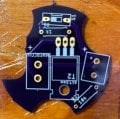
I have bread-boarded this, and the breadboard version on my workbench behaves precisely like I would expect it to. I have also produced a real board (thanks OSH Park!) from this design. Here's the board, also from Eagle, as manufactured by OSH.

Screenshot 2022-10-19 104736.jpg

As far as I can tell, it appears that my produced board matches my breadboard, which matches the circuit diagram that I have produced. But the circuit doesn't work:
- Expected behavior: passing a magnet near the magnetic reed switch should switch power, such that I should have 0VDC on output normally, and 12VDC on output when a magnet is near the switch.
- Achieved behavior: 12VDC is always provided to the output. The magnetic reed switch shows high resistance (~10Mohm) normally, and low resistance (<1ohm) with magnet nearby.

What am I doing wrong? What things can I look at to try to refine this problem?

Thanks,
Dan
 

DickCappels

Joined Aug 21, 2008
10,152
How do you know that it is not working?

Do you realize that under certain conditions your transistor may have a current gain of 2.3?

Please describe your load and its expected current drain.
 

Thread Starter

Daniel McMath

Joined Dec 28, 2015
50
Looks like you have the D and S terminals of the FET swapped. Why does your circuit include a 2N5496? The 2N5496 is a bipolar transistor, but the IRFB7546 is a MOSFET with a completely different pinout.
Do I have them switched? That would make me feel unusually silly, because I checked that like 6 times. Hmm... ignore for a moment what the label on the thing says -- it's actually an IRFB7546 -- and just look at where the wires go. Do I at least have this part right?
- Pin 1: Gate. Connects through a resistor to the switch.
- Pin 2: Drain. Connects to negative side of the load.
- Pin 3: Source. Connects to ground.

Understand the IRFB7546 is a totally different thing than the 2N5496, but they have the same footprint on the board, and it seemed simpler than creating a new library component. I'll admit that's causing some confusion here.
 

Thread Starter

Daniel McMath

Joined Dec 28, 2015
50
How do you know that it is not working?

Do you realize that under certain conditions your transistor may have a current gain of 2.3?

Please describe your load and its expected current drain.
Dick, it's supposed to be a switching circuit, but it isn't switching. Regardless of whether I have a magnet near the switch, I get 12VDC on output.

I had no idea the current gain could be as high as 2.3. I also don't have any idea what that means in this application, if I'm going to be honest.

The load is a heated vest; just a big resistor, really. Believe the manufacturer says that it wants something like 8A at 12VDC.
 

Thread Starter

Daniel McMath

Joined Dec 28, 2015
50
On the pcb you have it connected to the negative of the supply.
I don't see how that's true, I'm sorry. On the diagram, the INNERCONN component is the connection to the battery, which I understand to be the supply. The other connector, on the bottom of the board, is the load. I see the middle pin, which I read as Pin 2 / Drain, with a line to the negative terminal of the load connector. And the right-side pin, which I read as Pin 3 / Source, going to the negative terminal of the connection that goes to the battery.

But to test: I swapped the S and D on the breadboard, and I get power through the load all the time.

I'm obviously wrong -- my circuit doesn't work. I just don't see **how** I'm wrong. :( Board pictures attached.

Thanks,
Dan
 

Attachments

Thread Starter

Daniel McMath

Joined Dec 28, 2015
50
My bad. I've since deleted the post.
I don't think I would have deleted the post -- it looks like at least one other user was confused about precisely the same point, so having that documented for posterity seems valuable. Either way, your input is valuable to me and I appreciate the additional eyes on what should be a simple problem.

Still: the circuit doesn't behave like I'd expect it to. I'm doing something wrong, and it's probably both simple and obvious, but it's not coming together for me.
 

Ian0

Joined Aug 7, 2020
9,668
Looks like you have the D and S terminals of the FET swapped. Why does your circuit include a 2N5496? The 2N5496 is a bipolar transistor, but the IRFB7546 is a MOSFET with a completely different pinout.
It's not - it's like all power transistors - control pin on the left, output pin in the middle.
 

crutschow

Joined Mar 14, 2008
34,283
Okay, the layout does look correct to me.

Can you continuity check all the traces on a bare board to make sure it is connected exactly as the layout shows?

Also can you measure all the voltages on the board when it is operating incorrectly and note them on the schematic?
 

Thread Starter

Daniel McMath

Joined Dec 28, 2015
50
What is the voltage between source and drain (when it is meant to be off, and when it is meant to be on)?
On the breadboard (which works):
- 0VDC in the one case, 9.6VDC in the other

See below for table of voltages on the transistor

Which is really weird, because in both states, I'm getting 10.6VDC to the load. Also, the board gets hot very rapidly, so I guess I'll have to figure out a heat sink method.

To reply to crutschow, connectivity check appears to be consistent, e.g. 0ohms in all of the places that I expect it to be connected.

It'll take me a bit to get all the voltages for everything on the board in both states. I don't really have the right tools to do that properly, and it only works when I actually have the load connected, and the load, in this case, is a bulky object in my garage.
 
Last edited:

Thread Starter

Daniel McMath

Joined Dec 28, 2015
50
Ok, so voltage testing semi-successful. I slipped with a probe and made sparks, after which the behavior of the board changed, so I think I'll have to build out another one to do any more testing.

But here's what I have so far:
Input line seems to be doing the right thing -- it's 11V anywhere I expect it to be.
The switch seems to be switching -- it's 0 when there's no magnet near it, and 11V when I put the magnet on it.

For the transistor: (THESE VALUES ARE HIGHLY SUSPECT AND CANNOT BE DUPLICATED)
Switch Open (no magnet)Switch Closed (magnet)
G-D010.5
D-S0 (should be 11?)0.5
G-S011.1


Screenshot 2022-10-19 152110.jpg

The load is a heated vest, and it definitely starts heating up as soon as I connect it, with no magnet on the switch. Also, small correction to above -- the board gets hot (~95F) when the load is connected. With no load connected, it doesn't appear to be passing any current, so it does not heat up.
 
Last edited:

Thread Starter

Daniel McMath

Joined Dec 28, 2015
50
So I guess the conclusion of the community at this point is something like:
  • The diagram appears to be correct (despite the wrong transistor on the label)
  • The board layout appears to be correct
  • The result is wrong
  • Therefore: Dan assembled it badly

Does that sound like a reasonable up-shot of all this? Before I solder another round of parts into another board, I'd just like the common sense check that I haven't built something that's obviously stupid. It's easier to cut traces and install jumpers before I get the board populated, is all.
 

dl324

Joined Mar 30, 2015
16,845
Ok, so voltage testing semi-successful. I slipped with a probe and made sparks, after which the behavior of the board changed, so I think I'll have to build out another one to do any more testing.

But here's what I have so far:
Input line seems to be doing the right thing -- it's 11V anywhere I expect it to be.
The switch seems to be switching -- it's 0 when there's no magnet near it, and 11V when I put the magnet on it.

For the transistor:
Switch Open (no magnet)Switch Closed (magnet)
G-D010.5
D-S0 (should be 11?)0.5
G-S011.1
Your original complaint was that 12V was always being applied to the load.

Why are you measuring voltages between the MOSFET terminals? Measuring with respect to round is sufficient

We only need to know what the voltages on the gate and drain are. If you have things connected properly, the source will always be ground.

The drain-source voltage is an order of magnitude higher than it should be. 8A * 7.3mΩ = 58.4mV, you measured 500mV.
 
Top