 Facebook
 Google
 GitHub
 Linkedin
Folks,
I hope everyone is keeping well and best wishes for 2022.")
I am wondering can someone give me some guidance on this and I know thermal design is opening a whole can of juicy worms but I am using a particular switching converter IC and my power dissipation is not as good as I expect - its about 1Watt off the normal and I am getting 80 ish Percent efficiency as opposed to 90 - I am using a few mosfets but the power they are using doesn't account for the extra loss I am seeing.
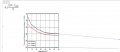
The datasheet has this graph and gives an example of expected Power dissipation from the datasheet and resulting copper required.
I am using around 1.2 Watts, this figure goes off the screen for a R theta value, it will be around 42 C/W - does that mean I need sufficient copper (ground) on my pcb to compensate for this figure?
I currently have 45cm2 of copper on my pcb ( solid ground fill) - 2 layers, I got the figure from Zuken design force on the area fill section. The graph makes no sense for low R theta values as the required copper will be huge
I am trying to see if increasing my copper area will improve the efficiency I am seeing, its not to be taken lightly as its a new board spin - from 2 layers to 4.
or am I talking nonsense...
I hope everyone is keeping well and best wishes for 2022.
I am wondering can someone give me some guidance on this and I know thermal design is opening a whole can of juicy worms but I am using a particular switching converter IC and my power dissipation is not as good as I expect - its about 1Watt off the normal and I am getting 80 ish Percent efficiency as opposed to 90 - I am using a few mosfets but the power they are using doesn't account for the extra loss I am seeing.
The datasheet has this graph and gives an example of expected Power dissipation from the datasheet and resulting copper required.
I am using around 1.2 Watts, this figure goes off the screen for a R theta value, it will be around 42 C/W - does that mean I need sufficient copper (ground) on my pcb to compensate for this figure?
I currently have 45cm2 of copper on my pcb ( solid ground fill) - 2 layers, I got the figure from Zuken design force on the area fill section. The graph makes no sense for low R theta values as the required copper will be huge
I am trying to see if increasing my copper area will improve the efficiency I am seeing, its not to be taken lightly as its a new board spin - from 2 layers to 4.
or am I talking nonsense...
Attachments
-
 58.6 KB Views: 4
Last edited:


