Hi Guys
Faced with a broken power supply...no volts out:-( i set about trying to repair.
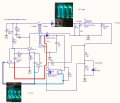
I sketched the circuit to the best of my ability and i think this is how it goes.[see attached]
After staring at the circuit for a few days and doing some comparisons with various textbooks on the subject it became more intriqing
Looking at the circuit it does not seem to be a forward converter as there is no diode from collector of the BUT11A to the HV rail.
C3 SHOULD BE 22 U 400V oops sorry i mis labelled,but it just has the rectified mains across it . The interesting parts are r2/c4 in parallel with the primary and hanging on the collector of Q1. AAAH is this then a parallel resonant circuit that is self starting and self oscillating?
I think it works as follows ...on switch on R3 TURNS Q1 hard on which charges C6/R6 and starts to remove the base drive from Q1 via Q2 collector.
The base of Q1 has just received a pulse from the secondary of T1 tertiary winding via C7...about 2V to enforce the turn on of Q1 and save some power.
Q1 continues to be turned off by Q2.and finally C4 R2 charge in the opposite direction as the collector of Q1 swings positive.
This is the inner loop. The outer loop is from the o/p and is fed back by the opto isolator to control the amount of drive to Q1.
If O/P volts go up U1 sinks more current setting the dc point of Q2 a little higher and throttling back Q1 slightly.
Anyway it turns out that there was no oscillation and hence no output as C7 had reduced in value to 50u, so i removed and fitted a new one and bingo we are in biz. C7 is fitted very close to the heatsink of Q1.....too close and it dries up.
If anyone has another idea of how this circuit works please let me know. What is bugging me though is the frequency it is working at and how you would set about designing this circuit. Putting the scope on the collector of Q1 revealed pulses running at about 67Khz which does not hold water with the jolly old "one over two pi root LC equals the resonant frequency". If i put in the numbers[i measured the inductance of all windings] and used the parallel resonance of T1 primary and R2C4 i end up with a resonance of 6.25KHZ a factor of 10 in error.
Can anyone offer an explanation of what i am doing wrong in my calcs and what topology this circuit is?
Can anyone point me in the direction of some design guides for this type of circuit as i think it should be a good circuit to use for 5v as well.
Can you leave the inductances as is and just change the reference on the output. maybe not.
Any information gratefully received.

 Facebook
 Google
 GitHub
 Linkedin


