 Facebook
 Google
 GitHub
 Linkedin
Hi,
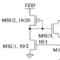
I am trying to build a bandgap reference circuit for my project. To do this, I have developed a startup circuit. I use a basic structure of startup circuit which can be seen below. The MSU2 represents resistor(diode connected load), MSU3 controls the rest of the circuit and MSU1 controls the gate of MSU2. I have understood the working principles of the circuits and arranged the W/L ratios as in the Figure. This circuit works when I set VDD to 3.3V. Drain of the MSU3 increases and gate of the MSU1 decreases.
The problem is my professor asks for two requirements. First one is that VDD must be around 1.2V. So, I assume I need to update W/L values based on this (probably increase the ratio of MSU2 to have a lower resistance). The other requirement is the circuit must settle after 3 us. If the only requirement would be voltage, then I could arrange that by changing ratios. However, I don't know how to make an arrangement for timing and satisfy both requirements. (I am neglecting the temperature for now). Any advice or source to read is going to help me a lot. Thanks for your help.
Attachments
-
 12.5 KB Views: 5


