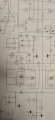
I have been trying to follow the EBC voltage from Q33 and Q30 -- and + side compairing each side as i went along, as it seems its the -- side of the sine wave not getting through, i tested relative to the 0v rail, (output resisters and sig gen connected) i think the fault may be further back in the circuit as both seem semetrical up to R74/ R60, although i am having trouble finding R60 to continue along the circuit
I seem to have good voltage across D30 and D28 to Q33 collector but after that nothing, the positive side is the same, am i working backwards?,
Is this schematic drawn in the usual positave to negative, Or is it drawn in the actual electron flow, as in negative to positave ?
To forward bias the base emitter junction of Q33 you will first have to get the amplifier working and drive it hard enough to have a current greater than about 3 amps in the load. Q30 and Q33 are to provide overload protection for the amplifier. When they conduct they shunt the drive to the emitter follower stages to prevent the amplifier from trying to provide more output current than it is designed to handle.
The first step in fault finding is study the schematic until you understand how it was designed to work.
To forward bias the base emitter junction of Q33 you will first have to get the amplifier working and drive it hard enough to have a current greater than about 3 amps in the load. Q30 and Q33 are to provide overload protection for the amplifier. When they conduct they shunt the drive to the emitter follower stages to prevent the amplifier from trying to provide more output current than it is designed to handle.
The first step in fault finding is study the schematic until you understand how it was designed to work.
When KISS says "the other side" I think he means the positive side of the left hand channel. I also think he means to keep one probe on the base of Q23 for all of the tests so as you progress through the tests you have the base emitter junctions in series.
I think with the resistors in that part of the circuit it will make it difficult to predict what the readings should be.
The polarity of the probes when testing the base emitter junction of Q40 will be the opposite way round as Q23 is NPN and Q40 is PNP.
Have the BC549Cs arrived yet ?
I don't understand your post #256. I don't see the connection between the protection circuits in the amplifier and the bias circuit.
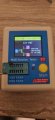
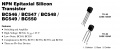
Your new transistor tester confirmed my suspicion that Q29 was faulty so it needs replacing. In the past I have seen transistors with the pinout not corresponding to the data sheet. First plug one of the new BC549Cs into your tester and confirm that the middle pin is the base. also confirm that the middle connection for the transistor on the board is the base. It may be marked on the board but if not confirm that is connected to the junction of R57 and R65. If so fit the new transistor. with now signal injected measure the voltage between the emitter and collector of Q29. I expect it to be between 3.6 and 4.2 volts. Report the results and we will tell you what to do next.
The transistor i tested was not from Q29, it was just an old one i had lying around,
However i will test a new one and post the picture of it in the teater, then replace Q29 with that one and test between emitter and collector and post my results
I forget we are dealing with a total newbie and I apologize. The junction of interest is the B-E junction. The polarity that it;s tested depends on the arrow. it's forward biased just like the arrow in a diode. That's the interested direction.
Silicon transistors, the value is around 0.6-0.7V, but it's not a gold specification. That diode is there all the time. I belive it changes -10mV/K. -10mV per Kelvin or degree C. The temperature scales have the same slope. Diodes can be used as temperature sensors. Their slope is a material property.
The B-E junction should test (diode-like) when the transistor is out of circuit. In circuit testing is always a pain, The diode-test on most DMM's really helped. The voltage the diode can read is limited which means it may not test LED's. We used to use resistance mode to try to test the junctions. The current source in an old VOM (Volt-OhmMeter) or what the DMM was called was usually a resistor and a 1.5V battery depending on the range.
This test in circuit depends on the components around it.
An in-circuit transistor checker generally depends on inversion. The transistor "works" if it inverts. It may not work properly, but it shows an active device.
Vce(SAT) is a controlled junction. It's the minimum voltage that is dropped across the C-E junction at high base current levels. It;s important when the transistor is being used as a switch.
We generally use the difference between the inverting and non-inverting inputs of an OP Amp to see if an OP amp is working. It doesn't work in all circuits.
The bias regulator.
You have to "overcome" the B-E voltage drop in order for the transistor to conduct. Without the bias regulator you get cross-over distortion. i.e. there would be a 0.6V of a flat sine wave where the signal crosses the zero axis.
The bias regulator provides a temperature compensated n*Vbe drop between the drive transistors plus a little extra to keep the output always conducting a little.
A low or zero bias regulator jsut means the amp has cross-over distortion.
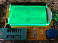
Ok, here is the photo of the NEW BC549C in the tester, i have now fitted this in Q29 position, the Base does connect to the junction of R57 and R65,
the voltage between the Emitter and Collector of Q29 is indeed 4.00vdc no load connected,
what would you like me to do next ?

 Facebook
 Google
 GitHub
 Linkedin
 494.5 KB Views: 4