simple BJT question

Thread Starter

MikeJacobs

Joined Dec 7, 2019
226
Reliving my circuit days and came across something I forgot

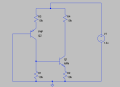
Say you had a massive nearly infinite current source. Maybe its a giant battery or similar.

You can this giant battery to the base of a simple npn but with no base resistor.
You connect the emitter with say a 500 ohm resistor to ground.

With no base resistor how do you determine what the base current is? AKA what is the base terminal input impedance?
Trying to understand what would dictate how much base current can be sunk if there is no base resistor to limit it.

Thanks
 

Thread Starter

MikeJacobs

Joined Dec 7, 2019
226
and I see above my stupid MacBook has auto corrected BJT to BUT making me look like an idiot again
I HATE SIRI :mad:

Moderator edit: Corrected thread title to "simple BJT question"
 

Thread Starter

MikeJacobs

Joined Dec 7, 2019
226
Also as a follow up
One thing I have always struggled with is "what drives what" in BJT circuits
let me see if I can explain.
In other words what are the hard constraints

So for example same as above question
Lets say you have the same npn and we know we have a .7 drop VBE.

Does that mean that we can force VB to 100% be .7 above VE or does it mean we can force VE to be .7 below VB
Which is the "enforcer" so to speak.
 

Thread Starter

MikeJacobs

Joined Dec 7, 2019
226
In other words, What parts of the BJT constrain the other. Its one thing to know BJT equations but another to have intuition

So I am seeking to understand what constrains what. In your answer you are telling me it will sink what it wants to sink.
That tells me that IB with no base resistor is constrained by IC and IE values.
Is that correct?

But then if that is true, then the VBE drop is what actually contains the base voltage.
And that is what I don't get

What parts constrain what. What governs what in a BJT
 

Papabravo

Joined Feb 24, 2006
21,158
Whatever happens the base can not be more than 0.7V above the Emitter.
Draw a circuit of what you have in mind. Words just don't make it when it comes to circuits.
 

crutschow

Joined Mar 14, 2008
34,280
The base-emitter junction of a BJT looks like a forward biased diode with a drop of about 0.7V when it's carrying a nominal current of a mA or so.
So if you understand diodes than you will understand the base-emitter junction.
 

MrChips

Joined Oct 2, 2009
30,706
In other words, What parts of the BJT constrain the other. Its one thing to know BJT equations but another to have intuition

So I am seeking to understand what constrains what. In your answer you are telling me it will sink what it wants to sink.
That tells me that IB with no base resistor is constrained by IC and IE values.
Is that correct?

But then if that is true, then the VBE drop is what actually contains the base voltage.
And that is what I don't get

What parts constrain what. What governs what in a BJT
The diode current and voltage is found by solving two equations, the diode equation and the resistor load line.

1594698212109.png

VDD is your supply voltage.
R is the resistor (base and emitter resistors added).
The diode current ID and diode voltage VD is called the Q-point (quiescent point) or operating point.
 

LvW

Joined Jun 13, 2013
1,752
MikeJacobs - perhaps yor problems in understanding result from the fact that you think that the base current Ib would determine/control the collector current Ic (and VBE would be the result of this current)?
No - the contrary is true.
The voltage VBE controls Ic (Shockleys famous equatiion) - and Ib is the result of Vbe.
However, Ib is - more or less - a fixed percentage of Ic - and therefore some people think that the equation Ic=B*Ib (resulting from Ib=Ic/B) would say anything about cause and effect. But that is a severe misinterpretation.
(As far as the base current is concerned, the great late Barrie Gilbert speaks about a "defect" and a "nuisance").
Remember the classical desogn of a common-emitter stage with a voltage divider for base biasing.
In some other cases, we have only one large resistor for base biasing - and it is common practice to speak about "current injection". But this is nothing else than "labour jargon". We cannot "inject" a current - instead, we have a simple voltage divider consisting of this resistor and the base-emitter path of the transistor which allows a dc voltage in the range 0.6...0.7 volts only.
 

Thread Starter

MikeJacobs

Joined Dec 7, 2019
226
Whatever happens the base can not be more than 0.7V above the Emitter.
Draw a circuit of what you have in mind. Words just don't make it when it comes to circuits.
Something like this perhaps.
Consider that configuration im not calling it a circuit because it lacks completeness

We don't know the base of voltage of Q2 because the base current of Q2 contributes to the overall current going through Q1
So what constrains what at this point?

thinking like a diode, which way are we clamped.

Is the base voltage guaranteed to to be .7 above the emitter? garunteeing that VB is a certain voltage which limits the current through R2?

Or is it the other way around.

Is the Ve voltage clamped to be .7 below whatever VB is? But how do we determine Vb.
 

Attachments

Thread Starter

MikeJacobs

Joined Dec 7, 2019
226
MikeJacobs - perhaps yor problems in understanding result from the fact that you think that the base current Ib would determine/control the collector current Ic (and VBE would be the result of this current)?
No - the contrary is true.
I would say you are correct here.
But how can you say that IB does not control IC

And that is the part I fail to grasp

The dc current gain of an NPN is IC = ib*beta

So very clearly the ib controls IC
Can you elaborate more? This may be why im confused.
 

Papabravo

Joined Feb 24, 2006
21,158
Your "configuration" is improbable because there is no voltage source for the collector of Q2. If Q1 is off there is no base current and Q2 will be off. If Q1 is on then so what there is still no voltage source for Q2 to work with. Why don't we try don't we try analyzing a real circuit instead of a random "configuration" as you put it.
 

LvW

Joined Jun 13, 2013
1,752
I would say you are correct here.
But how can you say that IB does not control IC

And that is the part I fail to grasp

The dc current gain of an NPN is IC = ib*beta

So very clearly the ib controls IC
Can you elaborate more? This may be why im confused.
Mike - an equation like Ic=ib*beta is a formula - nothing else. Such a formula never tells you something about cause and effect.
It results from Ib being a fixed part of Ic (determined by Vbe): Ib=Ic/beta.
I know there are some sources (primarily internet, even some books) which state that Ib would control Ic - but did you ever see something like a proof?
No - it is only a statement (based on the misinterpretation of the shown relation between Ib and Ic).
However, there are many proofs which clearly show that Ic (as well as Ib) are both controlled by Vbe.
Everybody knows how the pn-junction of the diode reacts upon a voltage between both nodes.
Is there any good reason why the pn junction within the transistor suddenly should behave differently?
What about Shockley`s exponential equation - not valid?
To me, it is really a "mystery" how somebody can believe that a small current (like Ib) should be able to control and determine a current that is 200...300 times larger.
Ask yourself how and why a current mirror or a Vbe multiplier works.
More than that, all the classical design rules for building a common emitter stage consider the fact the Ic is controlled by Vbe (RE-feedback, low-resistive base voltage divider).
There are many additional effects and observations (tempco -2mV/K; Early effect,...) which clearly show how Ic depends on Vbe only!!
(Comment: But I know - and I have learned - it is not easy to convince somebody who 40 or 50 years ago has learned the opposite).
 
Last edited:

Thread Starter

MikeJacobs

Joined Dec 7, 2019
226
Your "configuration" is improbable because there is no voltage source for the collector of Q2. If Q1 is off there is no base current and Q2 will be off. If Q1 is on then so what there is still no voltage source for Q2 to work with. Why don't we try don't we try analyzing a real circuit instead of a random "configuration" as you put it.
Sorry, it was meant to assume a common voltage source on the top rail. feeding both BJT's

Lets trying something simple like this.
Lets say the question is, how do we get the current going through Q1?
 

Attachments

MrChips

Joined Oct 2, 2009
30,706
Ic = β x IB

The problem is β is not a constant. It changes with Ic and from device to device, even within the same part number and manufacturing batch.

We do not use the value of β to determine Ic because we do not know the exact value of β.
We use a range of β to give worst case scenarios so that the circuit will work for all encountable values of β.

In order to design the circuit as a switch, we assume a worst case value of β = 10.
In an amplifier design, the transistor's β could be 300. Yet, we design the circuit with enough negative feedback so that with a moderate gain of 20, for example, the circuit will still function correctly even if the true β turns out to be 100 and not 300.
 

MrChips

Joined Oct 2, 2009
30,706
Sorry, it was meant to assume a common voltage source on the top rail. feeding both BJT's

Lets trying something simple like this.
Lets say the question is, how do we get the current going through Q1?
In your example given, whether or not Q1 is in saturation mode, the max current in Q1 is V1 / (R4 + R2).
With Q2 in saturation you still need to determine if Q1 is in saturation, cut-off, or in the linear region.
 

Thread Starter

MikeJacobs

Joined Dec 7, 2019
226
I know we generally don't know beta
And this is what is confusing. If we don't know beta how can we ever hand calculate some of these circuits
 

Thread Starter

MikeJacobs

Joined Dec 7, 2019
226
Mike - an equation like Ic=ib*beta is a formula - nothing else. Such a formula never tells you something about cause and effect.
It results from Ib being a fixed part of Ic (determined by Vbe): Ib=Ic/beta.
I know there are some sources (primarily internet, even some books) which state that Ib would control Ic - but did you ever see something like a proof?
No - it is only a statement (based on the misinterpretation of the shown relation between Ib and Ic).
However, there are many proofs which clearly show that Ic (as well as Ib) are both controlled by Vbe.
Everybody knows how the pn-junction of the diode reacts upon a voltage between both nodes.
Is there any good reason why the pn junction within the transistor suddenly should behave differently?
What about Shockley`s exponential equation - not valid?
To me, it is really a "mystery" how somebody can believe that a small current (like Ib) should be able to control and determine a current that is 200...300 times larger.
Ask yourself how and why a current mirror or a Vbe multiplier works.
More than that, all the classical design rules for building a common emitter stage consider the fact the Ic is controlled by Vbe (RE-feedback, low-resistive base voltage divider).
There are many additional effects and observations (tempco -2mV/K; Early effect,...) which clearly show how Ic depends on Vbe only!!
(Comment: But I know - and I have learned - it is not easy to convince somebody who 40 or 50 years ago has learned the opposite).
How does VBE have anything to do with it. VBE is constant at .7
 

LvW

Joined Jun 13, 2013
1,752
How does VBE have anything to do with it. VBE is constant at .7
Mike - this is a very simplified view (and wrong!). There will be current Ic (and Ib) even for values of Vbe=0.2..0.3 volts.
Have a look onto the classical diode characteristic I=f(Vd). The same applies to the transistor!
Vbe is not a constant! It is the controlling parameter.
However, normally we assume a value of APPROXIMATELY Vbe=0.7 volts. This a value which can be used for design purposes becaus we do not know better!!
The good amplification properties of the BJT result from the large sensitivity Of Ic against Vbe (exponential). For this reason, the temperature influence of Vbe plays an important role (for each degree temperature increase we must reduce Vbe by 2mV to keep Ic constant; this propety is a clear proff of voltage control).
For these rerasons, we make use of voltage feedback (emitter resistor RE). This feedback effect drastically reduces the influence of the (not exactly known) Vbe value.
Again: We clearly must distinguish between (a) physical properties (Vbe controls Ic) and (b) practical design rules for designing BJT circuits (we asume Vbe=0.65 or 0.7 volts for calculation purposes only!)

The attached drawing shows how an unknown value of the actual Vbe has only a minor influence on the resulting collector current.

"And this is what is confusing. If we don't know beta how can we ever hand calculate some of these circuits "
Example: Common emitter amplifier. The base voltage divider is designed as low-resistive as possible (with respect to power consumption and input resistance). Classical rule of thumb: Current through the divider chain at least 10 times larger than the estimated base current.
Why?
Because, in this case, the tolerances of Ib play a minor role for producing the wanted voltage at the base. For some rough calculations you even can NEGLECT the base current.
More than that: Two BJT-based amplifier stages (same DC operating point), but with two different beta-values (100 and 400) will have the same voltage amplification! No influence of beta or B on voltage amplification. It is only the transconductance d(Ic)/d(Vbe) which matters!
 

Attachments

Last edited:
Top