 Facebook
 Google
 GitHub
 Linkedin
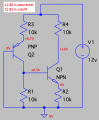
simple BJT question
- Thread starter MikeJacobs
- Start date


| Thread starter | Similar threads | Forum | Replies | Date |
|---|---|---|---|---|
|
|
Simple relay schematic question | General Electronics Chat | 14 | |
| R | LED lamp simple circuit question | General Electronics Chat | 5 | |
| D | Noob asking a simple question | Digital Design | 5 | |
| F | Simple question about “flash” used as verb | IC Design | 5 | |
| M | Simple Theoretical question, 3 things in parallel | General Electronics Chat | 39 |


