Facebook
 Google
 GitHub
 Linkedin
Hi everyone,
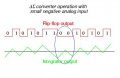
From the attachment, the block diagram shows the architecture of New Synchronous Voltage to Frequency Converter. Currently I am reading it's paper and it says :
At each conversion, the integrator keeps a running total of its previous output and its current input. The output from the integrator is feed to a 1-bit analog/digital converter (ADC). This is simply a comparator with its reference input at a level of half the input range, 0V in this case.
The ADC output feeds a 1-bit digital/analog converter (DAC) which has output levels equal +Ur or -Ur. A summing amplifier completes the loop by summing the current input signal and the previous sample DAC output. The aim of the feedback loop is to try to maintain the average output of the integrator at the comparator reference level 0V.
Honestly, I am quite confuse with the explanations and here are my questions:
1) How does the DAC works in the circuit since the output of the D-flip flop is only 1 or 0 and not a range of binary numbers?
2) Why are there +Ur and -Ur at the DAC and how it works from the diagram? I do understand how DAC works but don't know how it works from the attached picture.
3) Aren't the output of the comparator become 1 when the output integrator is more than 0V (which is the reference level) and become 0 when integrator output is less than 0V? Why it does not show the correct waveform at the output of D flip-flop as shown in Figure 3c?
4) What's one shot (OS) and how it works?
Appreciate if anyone could answer my questions, really need to know this before I can proceed to further topics. Thank you.
Attachments
-
 111 KB Views: 82
")