SiC Mosfet Vds Ringing

Thread Starter

slantoner

Joined May 16, 2018
10
Hi everyone,
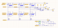
I created a circuit which contains ;
-1 input,4 isolated output SMPS for sic mosfet driver power supply.
-6 SiC mosfet , 6 schootky diode.
-4 United-chemicon Al-Elct. capacitors as 2 series and 2 parallels.Thus Vmax=900V Totalcap=1mF
-mosfet model: Littelfuse LSIC1MO120E0080
I'am trying my circuit part by part, Now I just set-up one driver one mosfet , four capacitors and smps rails.
In attachments, I shared my inverter stage.
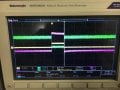
I just put 37R load from terminal A to DC- terminal, I charged to my capacitors around 30V and I applied 100us one pulse to mosfet. I'am adding scope picture.
Yellow:3.3V primary firing signal,
Purple:Vgs,
Green:Vds,

Why my Vds voltage is ringing like that ? The ringing time is about 60us and this is so huge ? Actually Thats different from ringing effect.
I also charged my capacitors to 330VDC but I saw the same kind of waveform with increased magnitude of course.

Do you have an idea about that ?
Really need help. If you have questions ask me please.
Thank you.
 

Attachments

shortbus

Joined Sep 30, 2009
10,045
Just some thoughts that apply to mosfets. What is the value of the gate resistor? Do you have gate to source resistors in the circuit? What is the distance(physical distance) between the gate drive device and the actual mosfet being used. Is the test circuit being done on a plastic bread board, or is it a soldered PCB even a Vero board will be better than a bread board.
 

Thread Starter

slantoner

Joined May 16, 2018
10
Just some thoughts that apply to mosfets. What is the value of the gate resistor? Do you have gate to source resistors in the circuit? What is the distance(physical distance) between the gate drive device and the actual mosfet being used. Is the test circuit being done on a plastic bread board, or is it a soldered PCB even a Vero board will be better than a bread board.
Shortbus,
Gate resistors,
Rturnoff=20ohm,
Rturnon=7ohm,
Its soldered PCB which includes everything on it.
Physical distance is 10cm as maximum.

Now I realized something, 37R load not exactly just a resistor ( I took it from someone) , It has self inductance. I tried with just 15R resistor now and everything is ok now,
Why RL load is affecting like that ? This circuit will also drive the RL load in this application ?
I added the result of 15R load.

How can fix these effect of RL ?
 

Attachments

ebp

Joined Feb 8, 2018
2,332
If you have inductance in the load then the inductance will resonate with FET capacitance and ring. The only way to prevent ringing is to provide some place for the energy stored in the inductance to go, which is what your diodes across the FETs will do - provided the ringing voltage is high enough.

For the diodes to be effective, the supply rails must be low impedance at high frequency. Even good quality electrolytic capacitors aren't very good at high frequency. The other problem is that there is usually some amount of inductance in the connections between the diodes and the capacitors. The unwanted inductance can be reduced by careful attention to layout to minimize "loop area" - the area bounded by the "out" and "return" paths for the current. It is often necessary to include some capacitors that perform well at high frequency physically close to where the capacitance is required. Depending on the amount of capacitance required and how much energy must go into them, ceramic capacitors may be sufficient (good at HF, but only small capacitance readily available at high voltage). Plastic film capacitors with "stacked" design (low inductance) may be more suitable. Polypropylene film-foil (as opposed to metalized film) perform quite well, though they are rather large and a bit expensive.

Be careful with electrolytic capacitors connected in series to achieve high voltage. If the capacitances aren't equal, you can get a serious imbalance of voltage between them. I haven't looked at it in detail, but the looks pretty good:
www.cde.com/resources/catalogs/AEappGUIDE.pdf
 

Thread Starter

slantoner

Joined May 16, 2018
10
The gate/source resistor should be much higher than that I use 10Kohm, but any thing above 2.2K will work.


10cm from driver to gate? Every App note I've ever read says to keep it less than 1"(25.4mm) Any longer allows ringing from parasitic's.
Hey,
sorry I did not mention; I used about 33kohm to gate-source resistor and yes gate device to mosfet gate way very large but I had to do that.

My main question is how can I fight with RL load ?
 

Thread Starter

slantoner

Joined May 16, 2018
10
If you have inductance in the load then the inductance will resonate with FET capacitance and ring. The only way to prevent ringing is to provide some place for the energy stored in the inductance to go, which is what your diodes across the FETs will do - provided the ringing voltage is high enough.

For the diodes to be effective, the supply rails must be low impedance at high frequency. Even good quality electrolytic capacitors aren't very good at high frequency. The other problem is that there is usually some amount of inductance in the connections between the diodes and the capacitors. The unwanted inductance can be reduced by careful attention to layout to minimize "loop area" - the area bounded by the "out" and "return" paths for the current. It is often necessary to include some capacitors that perform well at high frequency physically close to where the capacitance is required. Depending on the amount of capacitance required and how much energy must go into them, ceramic capacitors may be sufficient (good at HF, but only small capacitance readily available at high voltage). Plastic film capacitors with "stacked" design (low inductance) may be more suitable. Polypropylene film-foil (as opposed to metalized film) perform quite well, though they are rather large and a bit expensive.

Be careful with electrolytic capacitors connected in series to achieve high voltage. If the capacitances aren't equal, you can get a serious imbalance of voltage between them. I haven't looked at it in detail, but the looks pretty good:
www.cde.com/resources/catalogs/AEappGUIDE.pdf
I minimized the loop area by paralelling the DC- plane and DC+ plane rails and I also connected a plastic film capacitors at DC planes after the al-electrolytic capacitors ( close to mosfets) to minimize Al-electrolytic parasitics.
What do you think about snubbers for mosfet Vds ? If you used before, maybe you can share some values or design considerations ?
 

shortbus

Joined Sep 30, 2009
10,045
Hey,
sorry I did not mention; I used about 33kohm to gate-source resistor and yes gate device to mosfet gate way very large but I had to do that.

My main question is how can I fight with RL load ?
Now you're getting out of my knowledge level. But EBP gave you good advice. With inductive type loads, motors and such, you need to have bypass diodes.
 
Top