Facebook
 Google
 GitHub
 Linkedin
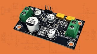
I'm not real sure what makes this one work. Pin 11 is supposed to be oscillator input, and 9 and 10 oscillator outputs... is this the feedback that was described in some places? Does R1/C1 determine the frequency of the oscillator? And what is the theoretical frequency? I'm not sure what order the stages go in, but I'm assuming the 1 Hz of the LED is because it's slowed down so many steps from the oscillator.This a counter-based solution mentioned before, based on something for another thread. The CD4060 is an CMOS oscillator and 14-stage divider. This means that the square wave at Q14 is 16,384 times slower than the oscillator frequency. This means that the for a time delay equivalent to the other circuits, the timing components can be 8192 times smaller. The 4060 is one of the greatest CMOS parts ever. However, it is standard CMOS so its output stage is good for only 1-2 mA and it cannot drive the SSR directly.
When the Q14 output is low, transistor Q1 is on and the SSR is on. I added an LED so you can see that the part is in the timing phase.
A closed switch holds the device in reset, so all outputs are low, the SSR is on, and the LED is off. When all switches are open, the oscillator starts and the LED starts blinking at about 1 Hz. After 8192 oscillator cycles, Q14 goes high. This turns off Q1 and the SSR, and freezes the oscillator through D1 (the 4060 does not have an enable/disable pin). When any switch closes it resets the counter, turning on the SSR.
C2 and R3 form a power-on-reset. When the circuit is powered on it runs through a 5 minute fan cycle even if all switches are open.
ak
View attachment 146929
If I wanted to omit the power on cycle, would I just leave out C2 and R3?