[S.T. 6 ] - BJT's characteristics

Thread Starter

PsySc0rpi0n

Joined Mar 4, 2014
1,762
Hi...

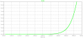
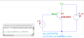
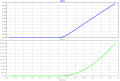
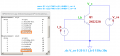
I'm trying to find the Early Voltage for a 2N2222 that I was expecting to be around 100V and I did this last year using the same bjt model in LTSpice and I found it to be 99.3V but I'm trying to do the same calcs now and I'm not close to this value. I'm finding it to be 73.3V and I can't figure out what's wrong.

We use the flat line equation y = mx + b to calculate Early Voltage using 2 data points given by LTSpice.
 

Attachments

Jony130

Joined Feb 17, 2009
5,488
Please plot this again but this time V_ce from -100V to 100V.


And are you sure that you have used the same model?
Notice that 2N2222A model has Vaf = 74.03V ??
.model 2N2222A NPN (Is=14.34f Xti=3 Eg=1.11 Vaf=74.03 Bf=255.9 Ne=1.307 Ise=14.34f Ikf=.2847 Xtb=1.5 Br=6.092 Nc=2 Isc=0 Ikr=0 Rc=1 Cjc=7.306p Mjc=.3416 Vjc=.75 Fc=.5 Cje=22.01p Mje=.377 Vje=.75 Tr=46.91n Tf=411.1p Itf=.6Vtf=1.7 Xtf=3 Rb=10 Vceo=40 Icrating=800m mfg=Fairchild)
But look at 2n2222 from Philips
.model 2N2222 NPN(IS=1E-14 VAF=100 BF=200 IKF=0.3 XTB=1.5 BR=3 CJC=8E-12 CJE=25E-12 TR=100E-9 TF=400E-12 ITF=1 VTF=2 XTF=3 RB=10 RC=.3 RE=.2 Vceo=30 Icrating=800m mfg=Philips)
 
Last edited:

Thread Starter

PsySc0rpi0n

Joined Mar 4, 2014
1,762
Yes, I was making a mistake. I was selecting 2N2222A instead of 2N2222.

Anyway, that problem is solved already.

Now I have another one.

Our teacher asked us to plot Ib(Vbe) in LTSpice for both 2N2222 and for 2N3055. The last one is a power bjt. I have noticed that in 2N2222, this plot gives the idea that in B-E junction we have a regular diode (Vγ≈0.7V) and and in 2N3055 this same voltage says ≈0.36V. I was wondering if this (or all) power bjt's are built with a schottky diode at the B-E junction.

Can you confirm or deny this?

Note: Our teacher already told us that regular bjt's has diodes in B-E junction.
2.3-plot.png is from 2N2222 and 2.4.3 is from 2N3055.
 

Attachments

Jony130

Joined Feb 17, 2009
5,488
No schottky junction in 2N3055. As you know 2N3055 is a power transistor with high current capacity. And this means that the junction area is much larger. And this is why Vbe is smaller for a given current. The Vbe of power transistors will start out at a smaller voltage at a low collector current of about 100 mA, but may increase substantially to 1 V or more at current in the 1A to 10A range.
Also notice that Ic = 10mA is very small current for a power transistor, so please increase your base current.
 
Last edited:

Thread Starter

PsySc0rpi0n

Joined Mar 4, 2014
1,762
No schottky junction in 2N3055. As you know 2N3055 is a power transistor with high current capacity. And this means that the junction area is much larger. And this is why Vbe is smaller for a given current. The Vbe of power transistors will start out at a smaller voltage at a low collector current of about 100 mA, but may increase substantially to 1 V or more at current in the 1A to 10A range.
Also notice that Ic = 10mA is very small current for a power transistor, so please increase your base current.

Sorry... Please specify the voltages you're referring to. You say that Vbe will start out at smaller voltage at a low Collector current. What is the smaller voltage you're referring to? Is it Vce?
I'm not understanding which depends on which?
From the attached plot I think that Vbe is dependant of Ib, because we have control over Ib (current source). But I'm not understanding this because I can see Vbe increasing no matter what Ib I have (I can't see Vbe depending on Ib).

Can you explain again what you explained in your previous post but using the attached plot?
 

Attachments

Last edited:

Jony130

Joined Feb 17, 2009
5,488
Sorry... Please specify the voltages you're referring to. You say that Vbe will start out at smaller voltage at a low Collector current. What is the smaller voltage you're referring to? Is it Vce?
I am sorry for the confusion. But I was trying to compare the Ic(Vbe) for a power transistor vs small signal transistor.
So , the Vbe of power transistors will start out at a smaller voltage (Vbe < 0.6V due to larger junction area) at a low collector current of about 100mA, compare to small signal transistor, but may increase substantially to 1V or more at current in the 1A to 10A range.
From the attached plot I think that Vbe is dependant of Ib, because we have control over Ib (current source). But I'm not understanding this because I can see Vbe increasing no matter what Ib I have (I can't see Vbe depending on Ib).
For me your plot looks normal. As for the BJT and "who has the control". There is no simple answer for this question. There two point of view/camps.
1. We treat BJT as a voltage controlled device (Ic depending on Vbe and base current fallows this relationship Ib = Ic/Hfe). Simply we treat BJT as an transconductance device.
2. We treat BJT as a current controlled device, an current amplifier (Ic depending on Ib).

In my opinion a BJT can be controlled either by voltage or current depending on the situation in circuit. Some circuit are more easily to explain using "voltage controlled" view but other circuit can be explain using using "current controlled" view.
 

Thread Starter

PsySc0rpi0n

Joined Mar 4, 2014
1,762
I am sorry for the confusion. But I was trying to compare the Ic(Vbe) for a power transistor vs small signal transistor.
So , the Vbe of power transistors will start out at a smaller voltage (Vbe < 0.6V due to larger junction area) at a low collector current of about 100mA, compare to small signal transistor, but may increase substantially to 1V or more at current in the 1A to 10A range.
So, when you say "So , the Vbe of power transistors will start out at a smaller voltage..." you mean that there will be (measurable) Ic when we have around 100mA of Ib?

For me your plot looks normal. As for the BJT and "who has the control". There is no simple answer for this question. There two point of view/camps.
1. We treat BJT as a voltage controlled device (Ic depending on Vbe and base current fallows this relationship Ib = Ic/Hfe). Simply we treat BJT as an transconductance device.
2. We treat BJT as a current controlled device, an current amplifier (Ic depending on Ib).

In my opinion a BJT can be controlled either by voltage or current depending on the situation in circuit. Some circuit are more easily to explain using "voltage controlled" view but other circuit can be explain using using "current controlled" view.
Ok, I think I got it now...

I was not understanding because I was not thinking about that only when the Base-Emitter junction is forward biased, when can have Ib flowing in that junction and making possible to have any Ic!
 

DickCappels

Joined Aug 21, 2008
10,171
This may or may not be helpful, but the way I would approach it would be to open the SPICE model file for that transistor and look for values for VAF (Forward early voltage) and VAR (Reverse early voltage). It isn't much fun but it would be a good way to check your answer.
 

Thread Starter

PsySc0rpi0n

Joined Mar 4, 2014
1,762
This may or may not be helpful, but the way I would approach it would be to open the SPICE model file for that transistor and look for values for VAF (Forward early voltage) and VAR (Reverse early voltage). It isn't much fun but it would be a good way to check your answer.
Already did hat but no info available in the spice model!
 

DickCappels

Joined Aug 21, 2008
10,171
Fairchild's model for the PN2222 is below, in case it can be of any help.

NPN (Is = 14.34f Xti = 3 Eg = 1.11 Vaf = 74.03 Bf = 255.9 Ne = 1.307 Ise = 14.34 Ikf = .2847 Xtb = 1.5 Br = 6.092 Isc = 0
Ikr = 0 Rc = 1 Cjc = 7.306p Mjc = .3416 Vjc = .75 Fc = .5 Cje = 22.01p Mje = .377 Vje = .75 Tr = 46.91n Tf = 411.1p Itf = .6
Vtf = 1.7 Xtf = 3 Rb = 10)
 

Thread Starter

PsySc0rpi0n

Joined Mar 4, 2014
1,762
Fairchild's model for the PN2222 is below, in case it can be of any help.

NPN (Is = 14.34f Xti = 3 Eg = 1.11 Vaf = 74.03 Bf = 255.9 Ne = 1.307 Ise = 14.34 Ikf = .2847 Xtb = 1.5 Br = 6.092 Isc = 0
Ikr = 0 Rc = 1 Cjc = 7.306p Mjc = .3416 Vjc = .75 Fc = .5 Cje = 22.01p Mje = .377 Vje = .75 Tr = 46.91n Tf = 411.1p Itf = .6
Vtf = 1.7 Xtf = 3 Rb = 10)
Thanks for that info!

Now I need to understand something else!

Our teacher is asking us, to simulate in LTSpice a power transistor as 2N2035. And he says to increase Ib and keep Vce at a certain value.
My question is:

How the hell we have a voltage drop of 0.7V at Base-Emitter junction if before we have this typical value (diode voltage drop) the current from the current source we have between Base and Emitter can't flow (until Vbe reaches 0.7V)???

I mean, if the current at the base can't flow between Base and Emitter because the diode in this juction is yet reverse biased, how does this voltage drop can exist in this junction?
 

Attachments

DickCappels

Joined Aug 21, 2008
10,171
When operating "normally" as a transistor, the base-emitter junction is forward biased. Otherwise, as you point out, there would be little other than leakage current flowing into the base terminal.
 

Jony130

Joined Feb 17, 2009
5,488
How the hell we have a voltage drop of 0.7V at Base-Emitter junction if before we have this typical value (diode voltage drop) the current from the current source we have between Base and Emitter can't flow (until Vbe reaches 0.7V)???
Simply, first replace 2N2222 with 2N3055 and change ".dc I_b 0 150u 1u" into "dc I_b 0 0.4 10u" .
 

WBahn

Joined Mar 31, 2012
30,057
Thanks for that info!

Now I need to understand something else!

Our teacher is asking us, to simulate in LTSpice a power transistor as 2N2035. And he says to increase Ib and keep Vce at a certain value.
My question is:

How the hell we have a voltage drop of 0.7V at Base-Emitter junction if before we have this typical value (diode voltage drop) the current from the current source we have between Base and Emitter can't flow (until Vbe reaches 0.7V)???

I mean, if the current at the base can't flow between Base and Emitter because the diode in this juction is yet reverse biased, how does this voltage drop can exist in this junction?
If you put a current source across the base emitter junction of a transistor then that source, because it is a current source, will produce whatever voltage is required in order to make that amount of current flow. That's what a current source does!
 

#12

Joined Nov 30, 2010
18,224
How the hell we have a voltage drop of 0.7V at Base-Emitter junction if before we have this typical value (diode voltage drop) the current from the current source we have between Base and Emitter can't flow (until Vbe reaches 0.7V)???
As far as I can tell, there is no zero in the Vbe/Ic function except when Vbe is forced to zero by you.
 

Attachments

Thread Starter

PsySc0rpi0n

Joined Mar 4, 2014
1,762
Before replying to you guys, just let me say that our teacher asked us to replace the 2N3055 for a complete spice model of Q2N3055.
The model he gave us is:

Code:
***********************************

.MODEL Q2n3055 npn
+IS=2.37426e-14 BF=129.119 NF=0.85 VAF=31.1252
+IKF=0.990922 ISE=2.47498e-10 NE=1.89002 BR=1.01252
+NR=0.924456 VAR=254.624 IKR=2.70227 ISC=2.47498e-10
+NC=2.90624 RB=3.66609 IRB=0.1 RBM=0.1
+RE=0.000352673 RC=0.0764459 XTB=1.34801 XTI=1.07207
+EG=1.206 CJE=9.03089e-08 VJE=0.513954 MJE=0.59999
+TF=1e-08 XTF=1.36696 VTF=1.02605 ITF=0.987296
+CJC=5e-10 VJC=0.400243 MJC=0.410238 XCJC=0.803124
+FC=0.661216 CJS=0 VJS=0.75 MJS=0.5
+TR=1e-07 PTF=0 KF=0 AF=1
* Model generated on Jan 24, 2004
* Model format: PSpice
The standard model was not complete and didn't allow us to find Early Voltage!.

Simply, first replace 2N2222 with 2N3055 and change ".dc I_b 0 150u 1u" into "dc I_b 0 0.4 10u" .
I already did that... But earlier today I spoke to my teacher and he told me that the 10mA would be enough to see what we need to see. But that we could use more base current and see what happens to hFE compared to 2N2222...
As far as I could understood from what he said, hFE should be quite lower in Q2N3055 than in 2N2222.

But yet about what we were supposed to confirm, that in small signal transistors Vbe is about 0.6V-0.7V and that in power transistors should be lower but I can't confirm that. Please check screens attached. When Ic = 100mA, Vbe is ≅ 0.63V. When can't I see Vbe lower than 0.6V in the simulaiton?

If you put a current source across the base emitter junction of a transistor then that source, because it is a current source, will produce whatever voltage is required in order to make that amount of current flow. That's what a current source does!
Today I got a little bit more confused about B-E junction. Is there or is not a diode in this junction? Or is just this junction's behaviour equivalent to a Si diode but no diode (physically) inside the transistor?

As far as I can tell, there is no zero in the Vbe/Ic function except when Vbe is forced to zero by you.
I'll ready that later as I need to finish this job ASAP! But thanks anyway!
 

Attachments

Last edited:

WBahn

Joined Mar 31, 2012
30,057
Are you comparing apples to apples?

What is Vbe for the two transistors when you have the same base current flowing in each?
 

Thread Starter

PsySc0rpi0n

Joined Mar 4, 2014
1,762
Are you comparing apples to apples?

What is Vbe for the two transistors when you have the same base current flowing in each?
What you mean? Sorry, I didn't understood.

I'm trying to check what my teacher told me. That hFE should be much lower in power transistors than in small signal transistors and also that Early Voltage is also lower (in terms of absolute values). This last one I could confirm but not the first one.

I'm suing this directive to try to find out the hFE but I don't know if it is correct!

Code:
.meas DC hfe Ic(Q1)/Ib(Q1)
This is returning 30 for all values of Ib that I'm testing!
 
Top