Facebook
 Google
 GitHub
 Linkedin
Hi...
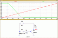
Our teacher asked us to simulate the right side of a circuit that is a NAND port. That right side of the circuit is attached.
I'm trying to prove with LTSpice that the attached circuit (which is part of a circuit that is supposed to work like a NAND port), knowing that Logic Level 0 is Vce between 0V and 1V and Logic Level 1 is Vce between 4V and 5V, needs to have such a Vbb that makes the transistor work within those limits for Level 0 and Level 1.
So, using the net equations for output and input, I have calculated Ic, then Ib and lastly Vbb for Logic Level 0 and Logic Level 1.
For Logic Level 1 I found Ic=455μA, Ib=2.27μA and Vbb=0.927V
For Logic Level 0 I found Ic=1.83mA, Ib=9.8μA and Vbb=1.61V
But if I try these values for Vbb in LTSpice, the Vbb=0.927V looks like OK because Vce < 1V which is OK for Logic Level 0, but for Vbb=1.61V I should get Vce>4V but LTSpice is outputing a value under 3.8V.
Is there anything wrong with my calcs or can it be due to Vbe of LTSpice to be lower than 0.7V???
Attachments
-
 13.6 KB Views: 35
 -
 6.8 KB Views: 35
 -
876 bytes Views: 14