Facebook
 Google
 GitHub
 Linkedin
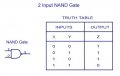
Before I answer to you, let me ask something about my own answer. I said that when both diode's cathodes are to +Vcc they are reverse biased, and therefor they are cut off and that D3 is also reverse biased beacuse voltage at anode and cathode is equal which is 0V. Now I think that this is not correct. If input diodes are cut off, I'll have a more positive voltage at the anode of D3 than at the cathode so it would be forward biased... Now I'm confused again!What about when one diode cathode is at 0V and the other is at Vcc?
Taking the case with both diodes at 0V and Vx=0.7V, if the diode D3 was removed, would the transistor be on or off? Do you need it to be on or off in this case? What does that tell you about the role of D3?
I'll reply to your 2 questions after I have solved this last question of mine!
 Is the simulation wrong?