Requesting some guidance on multi-voltage power distribution design

Thread Starter

ironhalo

Joined May 15, 2021
16
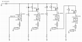
I am working on a design for the power distribution circuit of an upcoming EV project. The power source is a LiFePO4 pack that will operate in the 58V-80V range. I am using multiple dc-dc step-down regulators to support 24V, 12V, and 5V subsystems. I am planning to use p-channel mosfets as high-side switches to control each voltage subsystem so that I don't have to employ expensive/bulky physical switches with high power ratings. ( I'm intentionally doing high-side switching because many components throughout the overall design are chassis-grounded.) I have included in-line fuses for some added protection, however all of my dc-dc converters feature built-in over-current and over-voltage protection. My LiFePO4 BMS also features over-current and over/under-voltage prevention.

I have already tested each of my dc-dc converters with their respective loads, so I have indicated on the diagram what the max current draw for each part of the circuit should be. However I have not yet attempted any other calculations. Disclaimer: I have used BJTs and mosfets fairly regularly for both low-side and high-side switching, but only with regulated 12V supplies and 3V/5V micro controllers. This is my first time contemplating using FETs with voltage this high, or voltage that varies so widely over time.

So I'm hoping to get some general guidance on the direction I'm headed, and also on a few specific questions:

1) Given the fact that my battery pack's voltage will range from 58-80V over time, how do I make sure I am selecting a mosfet for PMOS1-PMOS3 that will function properly across this entire range? And once a proper mosfet is selected, what is the method for determining proper values for R1-R3 (again with respect to the wide voltage supply range)?

2) Would the diodes D1-D4 that I've included in my diagram be necessary to protect the mosfets in this design? Are dc-dc step-down converters the type of load that would create a need for such protection? (I have not used diodes to protect my mosfets in the past, but until now I have only switched simple 12V lighting circuits.)

3) I have learned that diodes are also commonly used to protect the gates of mosfets in some cases, but I don't fully understand what creates that requirement. Once a particular mosfet is selected, what is the math behind determining if gate protection is necessary?

Thanks in advance for any assistance.

Screen Shot 2021-06-11 at 8.08.26 PM.png
 

ronsimpson

Joined Oct 7, 2019
3,037
Most likely the P-MOSFET has a internal diode.
Many DC to DC power supplies have a shut down or enable function. This might save the MOSFETs.
A P-MOSFET sees voltage from S-G. It probably can not handle more than 20 volts. The way you have the switches 56 to 80 volts will be from G-S on the (now dead) FET.
 

crutschow

Joined Mar 14, 2008
34,412
You must always keep the gate-source voltage below its max rating (often 20V or less).
This can be done with a series resistor and a 10V Zener diode, for example.
 

Thread Starter

ironhalo

Joined May 15, 2021
16
Most likely the P-MOSFET has a internal diode.
Many DC to DC power supplies have a shut down or enable function. This might save the MOSFETs.
Good call, the 24v converter does have an enable pin, so that's one FET eliminated.

A P-MOSFET sees voltage from S-G. It probably can not handle more than 20 volts. The way you have the switches 56 to 80 volts will be from G-S on the (now dead) FET.
Ah, yes. Thanks.
 

Thread Starter

ironhalo

Joined May 15, 2021
16
Your final 5 volt converter has its source connected to negative...that's a no-no. (maybe just a schematic mistake?)
No it's being fed from the +12V output of the preceding converter. I relabeled it to make it a little more clear.
 
Last edited:

Thread Starter

ironhalo

Joined May 15, 2021
16
So now that I am no longer frying PMOS2 and PMOS3 (hopefully), back to my original question I guess... Given that my source voltage is ranging from 58-80V, can anyone teach me how to determine what combination of MOSFET specs and R values will result in reliable switching (and no burnt components)? FYI, switching speed is not a concern here.
 

ronsimpson

Joined Oct 7, 2019
3,037
From a DC point of view: In the data sheet there is a graph of "RDSon" & Vgs and some numbers on page 1. For transistor 4 you have 12 volts to turn on the part. At 12Vg-s the transistor will look like a resistor of 0.xx ohms. Simple math 0.xx ohms and 15A = ? watts and ? volts across the d-s. Skip over the data "100 watts" and find "100C/watt". Find out how hot the part will get. You know watts and temperature rise with no heat sink. With this you can know if you need to bolt the transistor to a piece of metal.

I would go to digikey.com or mouser.com and search for "mosfet", then "P" then 100V to 250V, then 20A & larger, then not surface mount? ....... then in-stock..... so pick one and lets review the numbers.
 

LowQCab

Joined Nov 6, 2012
4,064
Think of MOSFET Gates as a very small Capacitor that you must charge-up, or dis-charge.
This Capacitor is always connected between the "Gate" and the "Source" Pins.
All FETs have Voltage-Limits which will result in the Magic-Blue-Smoke getting out if you exceed them.
Most FET Gates are rated between ~10V and ~20V, a few go as high as ~30V.

Look at the Spec-Sheet for your FETs, find the largest Gate-Capacitance number from the graphs,
( this is not 100% accurate but is close enough to understand what's going on),
then, using an online calculator, like this one ........
http://referencedesigner.com/rfcal/cal_05.php
figure out the Resistor required to "Switch" the FET-Gate in an acceptable period of time.

There are times when increasing the Resistance,
( taking more time to completely "switch" ) can be an advantage.
Slower switching speed creates fewer problems with high Current-Surges or Voltage-Spikes,
which may be created if the switching times are too fast.
Probably the very slowest you would ever need to go to insure switching stability is
roughly 0.25-Seconds, ( 250ms ), and
0.05-Seconds, ( 50ms ), will be fine in most simple Power-Supply-switching situations.
Extremely Inductive or Capacitive Loads may benefit from longer time periods,
but be careful of the huge amount of Heat generated between full-On and full-Off.

Warning,
long high-Impedance wires can easily pick-up external Electrical "Noise" and cause serious headaches.
Keeping long-wire Impedances below ~1000-Ohms is good practice, lower is better.
If a higher Impedance is advantageous,
convert from a low-Impedance, to a higher Impedance, only at the very end of the long run.

Never allow a Gate to "Float" in a very high-Impedance condition, EVER, at any time.

When a FET is used as an "ON-OFF" Switch, the Gate Voltage should be either "0" or ~12V to ~15V,
if the Voltage is allowed to vary between ~0 and ~12, the FET will be somewhere between
fully "On", and fully "Off", this means that it will be acting as a "Variable-Resistor", and may
quickly generate a tremendous amount of Heat, possibly enough Heat to smoke it.
When a FET is fully "On", it still has a certain amount of Resistance, this is called its "RDS/On" Spec,
( Resistance-Drain-to-Source ) and is usually measured in Thousandths of an Ohm, ( mOhms ).
You can guesstimate the amount of Power that will be converted to Heat by multiplying
the Current flowing through the Circuit, by the "RDS/On" value,
example: 8-Amps X 0.030-Ohms-RDS/On = 0.24-Volts,
now that you have the Voltage number,
you can then calculate the Power that will be dissipated by the FET by
multiplying 8-Amps X 0.24-Volts = 1.92-Watts of Heat-Dissipation.
~2-Watts of Heat-Dissipation is too much for a small "TO-220" Transistor-Package by its self,
so you must mount it to a Heat-Sink to get rid of the excessive Heat.

BTW ................
Switching-Power-Supplies generally loose efficiency as the differences between the
Input-Voltage, and Output-Voltage, increases.
If you can lower your Battery Voltage, you will probably increase the System's efficiency.
.
.
.
 

AnalogKid

Joined Aug 1, 2013
11,037
A good rule of thumb for long term reliability is to operate all electronic components at 50% or less of their ratings.

For an 80 V peak input, use FETs rated for 150-200 V.
For a 5 A load, use FETs rated for at least 10 A.
For 1/8 W power dissipation in a resistor, use 1/4 watt parts.
etc.

Power MOSFETs have a fairly large gate capacitance. For the gate circuits, the resistors are a tradeoff between power dissipation in the resistors versus a low Thevenin equivalent resistance for the R-C circuit formed with the gate capacitance. The larger this time constant, the slower the FET will turn on and off. Example:

R1 = 10K, R2 = 47K, Cgs = 3000 pF (yes, many datasheets list it that way)

With no zener diode, at 58 V, Vgs = -10.1 V; at 80 V, Vgs = -14 V. Both are well within the normal 20 V range for Vgs, so - IF IF IF you trust that 80 V peak value - you don't need the zener. However, you might keep the zener in there to protect against R1 opening up.

The equivalent resistance at the gate is 8.25 K when turning on, and 10 K when turning off. With a 3000 pf gate capacitance, the worst-case is a time constant of 30 us. Three time constants (95%) is less than 1 ms, fast enough that the power dissipation spike as the FET goes from off to enhanced is too short to damage the device.

At 80 V input, power in the resistors is 113 mW and the current is 1.4 mA, so quarter-watt resistors should be fine.

If the circuit is in a high noise environment, you might want to scale down the resistor values to lower the circuit's susceptibility to radiated noise. If you do, keep an eye on the power dissipation.

ak
 
Last edited:

Thread Starter

ironhalo

Joined May 15, 2021
16
Many thanks to you all for your detailed instruction. I'm learning a lot about what I need to know for my applications.

I have taken the opportunity to simplify the circuit over the weekend. I now have a 5V converter with a shutdown pin, and have decided not to have discrete shutdown for my two 12V converters. Thus I have reduced the MOSFET count down to one. One lone PMOS that will switch the 58-80v source on/off for all branches. So at the present system load it would be switching 7A max, but for future growth I think I should round that up to 10A. So as suggested I'm looking at PMOS with 20A capacity or higher. I'm attaching a spreadsheet of the ones I can currently find in-stock.

So using the IXTQ26P20P as an example... Let's say I add more load in the future and I'm switching 10A max. So 10A x 170mOhm = 1.19V. Then 10A x 1.19V = 11.9W of heat dissipation. RthJA is used to get the FET's rise in temp without a heatsink, correct? As you can see in my spreadsheet, IXYS doesn't list RthJA, they only list RthJC and RthCS. But I assume it's a moot point because not even the TO-3P packaged devices will be able to dissipate 12W without a heatsink?

So then which of the remaining Rth values do I use to calculate heatsink requirements?

Screen Shot 2021-06-15 at 11.37.23 AM.pngScreen Shot 2021-06-14 at 1.27.59 PM.png
 

Thread Starter

ironhalo

Joined May 15, 2021
16
Switching-Power-Supplies generally loose efficiency as the differences between the
Input-Voltage, and Output-Voltage, increases.
If you can lower your Battery Voltage, you will probably increase the System's efficiency.
Thanks for all the input. The main battery voltage is dictated by the EV traction system, these step-down branch circuits are all ancillary. I considered running a separate lower voltage battery for my electronics, which I may do on future projects, but don't really want to hassle with fitting and charging 2 different batteries on this one.
 

crutschow

Joined Mar 14, 2008
34,412
So 10A x 170mOhm = 1.19V. Then 10A x 1.19V = 11.9W of heat dissipation.
If you used one of those with 85mΩ, you would cut the dissipation in half.
IXYS doesn't list RthJA, they only list RthJC and RthCS.
The power dissipation of most power packages to free air usually no more that a watt or so for typical ambients (for example the first listing shows the TO-3 has a 40°C/W RthJA).
Above that you need a heatsink.
 

Thread Starter

ironhalo

Joined May 15, 2021
16
Ha. That would be me upsizing my load from 7A to 10A in a hurry and not redoing my math. Let’s try that again.

10A x 170mOhm = 1.7V and 10A x 1.7V = 17W of heat dissipation. So even more implausible without a heatsink.

But going with the 48A FET I found…
10A x 85mOhm = .85V and 10A x .85V= 8.5W. Seems like the smarter choice with half as much heat to get rid of. That one also has a lower RthJC, which i assume will help if that is the coefficient used for calculating heat sink requirement?
 
Last edited:

Thread Starter

ironhalo

Joined May 15, 2021
16
Yes.
You add that to the heatsink thermal resistance to get RthJA
Okay, so working backwards, to keep the FET under 150C in a max ambient temp of 35C...

150C = 35C + 8.5W( .27 + Rth_of_heatsink ) ... So I would need a heatsink with an Rth of 13.26 C/W or lower?
 
Top