Request for a 5W transistor controlled LED flash light controller circuit review

Thread Starter

Hasan2019

Joined Sep 5, 2019
210
Hi there,

I wanted to get good explanation of this LED flasher circuit. Take a look on the attachment.
Vin=7.2V(max), Vout=6.8v (max), It has a big cap 1F at C2, and a switch for when charged and discharged ?
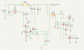

Transistor_based_led_driver.PNG


Power and protection stage

1. Connector J1 → BR1 (MB6S) : Full‑wave rectifies the AC input to DC.

2. C3, C4 (1000 µF) : Bulk smoothing of the rectified DC to reduce ripple.

D1 (2BZJ6.8Cxx zener) ; Creates a regulated low‑voltage rail (≈ 6.8 V) for the control circuitry, dropping and stabilizing from the rectified mains DC?

C5 (0.1 µF) : High‑frequency decoupling on the low‑voltage rail?

So:
Rectified mains → smoothed DC → zener‑regulated low‑voltage supply for the transistor logic, while the high‑voltage DC side ultimately feeds the LED load via the power transistor.


Control and flashing logic (Q1–Q4, R5–R10, C2)
You’ve got four S8550 PNP transistors (Q1–Q4) plus small‑signal diodes D2, D3 and a timing capacitor C2:

Q1–Q4 (S8550 PNP) These form the control logic, most likely an astable or monostable arrangement that periodically drives Q5.?

R5, R7 (150 Ω) : Base/emitter resistors that set base current and protect the transistors?

R6, R8, R9, R10 (5.1 kΩ) Bias and timing resistors—these, together with C2, define the charge/discharge paths that create the flashing period?

C2 (470 µF)
Main timing capacitor. Its charge/discharge through the 5.1 kΩ network sets the on/off duration.

D2, D3 (1N4148) Steering diodes that shape the timing—often used to make asymmetric charge/discharge paths (different ON and OFF times)?


Find out its working and benifits.
 

wayneh

Joined Sep 9, 2010
18,170
I wanted to get good explanation of this LED flasher circuit.
Why? Do you want to build it? Where did it come from? There are a lot of useless garbage schematics out there on the internet. It may be better to start by sharing what your goal is.
It has a big cap 1F at C2...
A 1F capacitor just to make a flashlight flash?! That's a red flag. I have a handful of flashing flashlights and not one has a big capacitor in it.
1. Connector J1 → BR1 (MB6S) : Full‑wave rectifies the AC input to DC.
I'm not seeing that. D1 is configured to short the input to ground whenever the voltage on pin 1 of J1 exceeds 0.7V above ground.

2. C3, C4 (1000 µF) : Bulk smoothing of the rectified DC to reduce ripple.
They're in parallel, so could be replaced by a single larger cap. Why does the circuit require that much smoothing capacity?

D1 (2BZJ6.8Cxx zener) ; Creates a regulated low‑voltage rail (≈ 6.8 V) for the control circuitry, dropping and stabilizing from the rectified mains DC?
D1 is not a zener as drawn. I believe you mean D2? I haven't looked it up but it appears to be a double zener? I don't pretend to understand this schematic but that portion of the circuit appears to be placing a load on the output that varies with the AC input, so perhaps it's meant as a smoothing filter. What is Q2 doing?

C5 (0.1 µF) : High‑frequency decoupling on the low‑voltage rail?
Sounds right.

That's as far as I got for now.
 

MisterBill2

Joined Jan 23, 2018
28,403
I would hesitate to call it a "flasher circuit." It contains a lot that does not seem to be related to flashing anything.
The portion that seems to be intended as a power input section is a bit random, to use a polite term.
 

Thread Starter

Hasan2019

Joined Sep 5, 2019
210
Why? Do you want to build it? Where did it come from? There are a lot of useless garbage schematics out there on the internet. It may be better to start by sharing what your goal is.
A 1F capacitor just to make a flashlight flash?! That's a red flag. I have a handful of flashing flashlights and not one has a big capacitor in it.
I'm not seeing that. D1 is configured to short the input to ground whenever the voltage on pin 1 of J1 exceeds 0.7V above ground.

They're in parallel, so could be replaced by a single larger cap. Why does the circuit require that much smoothing capacity?

D1 is not a zener as drawn. I believe you mean D2? I haven't looked it up but it appears to be a double zener? I don't pretend to understand this schematic but that portion of the circuit appears to be placing a load on the output that varies with the AC input, so perhaps it's meant as a smoothing filter. What is Q2 doing?

Sounds right.

That's as far as I got for now.

I have some modifications now,

1791634235117.png


It is powered by a wheel driven dynamo, rectifying it and charging a supercapacitor and using that to power a simple oscillator.

1. BR1 connection is corrected.
2. Pin4 of BRI is connected to GND of C4,C5
3. At SW1 R8 and R11 should meet together and other pin should to to GND.
4. D3 should connect to emitter of the Q4.
5. Now the output of Q6 can control Q3 and Q4


Here’s the entire circuit in one clean explanation:
  • BR1 + C3/C4/C5 create the main DC supply.
  • C2 + R6/R8/R9/R10 + D2/D3 form the timing oscillator.
  • Q1 + Q2 amplify the timing waveform.
  • Q6 is the master controller that drives Q3 and Q4.
  • Q3 + Q4 form a push‑pull pair that shapes ON/OFF transitions.
  • Q5 is the high‑current MOSFET that actually powers the LED.
  • SW1 selects between flashing mode and steady mode.
  • J2 outputs the controlled LED power.
 

Alec_t

Joined Sep 17, 2013
15,158
1) Is it an AI generated circuit? It looks like typical AI stuff that has numerous errors.
2) What are the output voltage and current capabilities of your dynamo?
3) What flash rate and duty cycle do you want?
4) Where does Vout appear?
5) Why does Q6 have no collector supply voltage?
6) Two components are labelled D2.
7) What is the intended purpose of the double zener diode (D2)?
8) Why does Q2 have both base and emitter grounded?
9) Q5 drain should not be fed from Q4 base
10) .......etc
 
Last edited:
You posted in another groups. I posted my thoughts on a very different way over there.

I can't see what you want but it looks like you have a full wave rectifier. This is how it should be connected. Pin 1 is +, Pin 2 is GND, Pins 3,4 are AC input.
1791645903697.png1791645953252.png
It might help to describe what functions you want.
Input is AC or DC 7.2V. Is this from a battery? or a regulated supply?
Output is DC 6.8V to drive a LED at 400mA. ? Driving a LED is more complicated than just giving it 6.8V. More later.
Flash rate is ?
What is the part number of the LED.
 

Thread Starter

Hasan2019

Joined Sep 5, 2019
210
You posted in another groups. I posted my thoughts on a very different way over there.

I can't see what you want but it looks like you have a full wave rectifier. This is how it should be connected. Pin 1 is +, Pin 2 is GND, Pins 3,4 are AC input.
View attachment 372095View attachment 372096
It might help to describe what functions you want.
Input is AC or DC 7.2V. Is this from a battery? or a regulated supply?
Output is DC 6.8V to drive a LED at 400mA. ? Driving a LED is more complicated than just giving it 6.8V. More later.
Flash rate is ?
What is the part number of the LED.
1791646594019.png
I was following this symbol as datasheet stated. I think this circuit has both option, battery and bi cycles dynamo that comes from tire ring. RC determines the flash rate. No idea about LED part number.

Anyway you wrote a long paragraph in the other forum about it, I need some time to readt it.
 
Last edited:
LEDs are not a "voltage" device but a current device. Current = light.
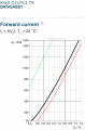
If you put 1A on this LED the voltage across the LED typically would be 6.61V but could be 6.75V or as little at 5.6V.
1791659304054.png
Here is a graph showing in back what the typical voltage & current is.
If 6.61V is put on a typical LED it will draw 1.0A. But could be as low at 850mA or as high as 2A.
When you get the LEDs form a good source, they should be close to typical. If you get the LEDs from Ebay.com or some questionable source they likely will be at or just beyond the red line or too close to the green line.
What I am trying to say is that the data sheet has information that many people do not understand.
1791659496360.png
If you are going to run your LED at 5Watts you need a really good heatsink!

For those that are learning about LEDs:
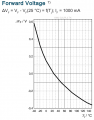
This graph shows at -40C the LED will need 0.6V more and at 100C it will want 0.25 volts less.
If you put the constant 6.61V on the LED and run at 1A with no heat sink the LED will get to 140C very fast and by then it will pull 1.4A and burn out.
1791660343464.png
 

Thread Starter

Hasan2019

Joined Sep 5, 2019
210
LEDs are not a "voltage" device but a current device. Current = light.
If you put 1A on this LED the voltage across the LED typically would be 6.61V but could be 6.75V or as little at 5.6V.
View attachment 372107
Here is a graph showing in back what the typical voltage & current is.
If 6.61V is put on a typical LED it will draw 1.0A. But could be as low at 850mA or as high as 2A.
When you get the LEDs form a good source, they should be close to typical. If you get the LEDs from Ebay.com or some questionable source they likely will be at or just beyond the red line or too close to the green line.
What I am trying to say is that the data sheet has information that many people do not understand.
View attachment 372109
If you are going to run your LED at 5Watts you need a really good heatsink!

For those that are learning about LEDs:
This graph shows at -40C the LED will need 0.6V more and at 100C it will want 0.25 volts less.
If you put the constant 6.61V on the LED and run at 1A with no heat sink the LED will get to 140C very fast and by then it will pull 1.4A and burn out.
View attachment 372110
Really interesting information
I have never thought about it before.

All components are SMT type in this PCB, the manufacturer may have good production number for business but market is competitive for sure , it's a cheap PCB. For cheap solution they have not use any CMOS. I can guess these are not very special LED's, brightness is good and in one module several LED's are combined. No idea about the sustainability of this circuit, you could tell it's a baby toy item.

Your knowledge based discussion says ' it's a silly story but could have been made some money.
 

WBahn

Joined Mar 31, 2012
33,253
It's a "baby toy item" that beings in mains voltage and flashes a 5 W LED?

It has mains voltage, but at the same time is driven by a wheel driven dynamo? On a baby toy?

All components are SMT, including a 1 farad capacitor?
 

Thread Starter

Hasan2019

Joined Sep 5, 2019
210
It's a "baby toy item" that beings in mains voltage and flashes a 5 W LED?

It has mains voltage, but at the same time is driven by a wheel driven dynamo? On a baby toy?

All components are SMT, including a 1 farad capacitor?
It's upto you how you will treat it. Big caps are though hole.
 
circuit is useless and makes no sense. plus it is drawn wery awkward.. R3,R4 are in parallel with R5 but places far away, with additional line crossings. placing three equal low value resustoprs in parallel would suggest there is high current through them, but it cannot be - at lest not from what you have drawn. because there are exactly three paths leading to this resistor back:
a) R7 which is way to high and would limit such current.
b) Q5 which is also a dead end - C1 can be charged by currents through R9 and R2. both of which are way too high to make any difference for three 5.1 Ohm resistors in parallel.
c) Q2 which is completely dead - no current flows through here.
next, D1 is a dead short for reverse polarity. so connecting AC to J1 would blow it up.
SW2 and everything right of it does nothing. when SW2 is in position:
1. current through R8 has nowhere to go. on one side is insulator (gate of Q5), and the other is through Q3 with nothing to drive its base.
2. not connected to enything so - nothing.
3. R11 conly connect to C2. 1uF make no difference anyway since it would be in parallel with C3 and C4 which are 2000x larger capacitance.
finally there is no load. for any circuit to do something, there meed to be some sort of load or "business end". this circuil lacks scuh thing. if J2 is meant as place to connect load (like 5W LED), then i am sorry to dissapoint you, R7 is a major problem to getting those 5W out.
 
It is quite a relief to see that a lot of other folks also saw a lot f flaws in the circuit.
It is more like a youngster who is good with pencils got hold of a symbol template and drew .............
BUT I dont want to offend the moderators so no critical remarks
 

Thread Starter

Hasan2019

Joined Sep 5, 2019
210
circuit is useless and makes no sense. plus it is drawn wery awkward.. R3,R4 are in parallel with R5 but places far away, with additional line crossings. placing three equal low value resustoprs in parallel would suggest there is high current through them, but it cannot be - at lest not from what you have drawn. because there are exactly three paths leading to this resistor back:
a) R7 which is way to high and would limit such current.
b) Q5 which is also a dead end - C1 can be charged by currents through R9 and R2. both of which are way too high to make any difference for three 5.1 Ohm resistors in parallel.
c) Q2 which is completely dead - no current flows through here.
next, D1 is a dead short for reverse polarity. so connecting AC to J1 would blow it up.
SW2 and everything right of it does nothing. when SW2 is in position:
1. current through R8 has nowhere to go. on one side is insulator (gate of Q5), and the other is through Q3 with nothing to drive its base.
2. not connected to enything so - nothing.
3. R11 conly connect to C2. 1uF make no difference anyway since it would be in parallel with C3 and C4 which are 2000x larger capacitance.
finally there is no load. for any circuit to do something, there meed to be some sort of load or "business end". this circuil lacks scuh thing. if J2 is meant as place to connect load (like 5W LED), then i am sorry to dissapoint you, R7 is a major problem to getting those 5W out.
Did you see the modified one @panic mode ?
I will check your comment.
 
Top