Facebook
 Google
 GitHub
 Linkedin

Hi there,
I wanted to get good explanation of this LED flasher circuit. Take a look on the attachment.
Vin=7.2V(max), Vout=6.8v (max), It has a big cap 1F at C2, and a switch for when charged and discharged ?
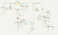
Power and protection stage
1. Connector J1 → BR1 (MB6S) : Full‑wave rectifies the AC input to DC.
2. C3, C4 (1000 µF) : Bulk smoothing of the rectified DC to reduce ripple.
D1 (2BZJ6.8Cxx zener) ; Creates a regulated low‑voltage rail (≈ 6.8 V) for the control circuitry, dropping and stabilizing from the rectified mains DC?
C5 (0.1 µF) : High‑frequency decoupling on the low‑voltage rail?
So:
Rectified mains → smoothed DC → zener‑regulated low‑voltage supply for the transistor logic, while the high‑voltage DC side ultimately feeds the LED load via the power transistor.
Control and flashing logic (Q1–Q4, R5–R10, C2)
You’ve got four S8550 PNP transistors (Q1–Q4) plus small‑signal diodes D2, D3 and a timing capacitor C2:
Q1–Q4 (S8550 PNP) These form the control logic, most likely an astable or monostable arrangement that periodically drives Q5.?
R5, R7 (150 Ω) : Base/emitter resistors that set base current and protect the transistors?
R6, R8, R9, R10 (5.1 kΩ) Bias and timing resistors—these, together with C2, define the charge/discharge paths that create the flashing period?
C2 (470 µF)
Main timing capacitor. Its charge/discharge through the 5.1 kΩ network sets the on/off duration.
D2, D3 (1N4148) Steering diodes that shape the timing—often used to make asymmetric charge/discharge paths (different ON and OFF times)?
Find out its working and benifits.
I wanted to get good explanation of this LED flasher circuit. Take a look on the attachment.
Vin=7.2V(max), Vout=6.8v (max), It has a big cap 1F at C2, and a switch for when charged and discharged ?
Power and protection stage
1. Connector J1 → BR1 (MB6S) : Full‑wave rectifies the AC input to DC.
2. C3, C4 (1000 µF) : Bulk smoothing of the rectified DC to reduce ripple.
D1 (2BZJ6.8Cxx zener) ; Creates a regulated low‑voltage rail (≈ 6.8 V) for the control circuitry, dropping and stabilizing from the rectified mains DC?
C5 (0.1 µF) : High‑frequency decoupling on the low‑voltage rail?
So:
Rectified mains → smoothed DC → zener‑regulated low‑voltage supply for the transistor logic, while the high‑voltage DC side ultimately feeds the LED load via the power transistor.
Control and flashing logic (Q1–Q4, R5–R10, C2)
You’ve got four S8550 PNP transistors (Q1–Q4) plus small‑signal diodes D2, D3 and a timing capacitor C2:
Q1–Q4 (S8550 PNP) These form the control logic, most likely an astable or monostable arrangement that periodically drives Q5.?
R5, R7 (150 Ω) : Base/emitter resistors that set base current and protect the transistors?
R6, R8, R9, R10 (5.1 kΩ) Bias and timing resistors—these, together with C2, define the charge/discharge paths that create the flashing period?
C2 (470 µF)
Main timing capacitor. Its charge/discharge through the 5.1 kΩ network sets the on/off duration.
D2, D3 (1N4148) Steering diodes that shape the timing—often used to make asymmetric charge/discharge paths (different ON and OFF times)?
Find out its working and benifits.