It depends on what your circuit does. If you want to be faithful to the apple-1 design that solution will do the trick. If you want to use SRAM like I did on an old video display then the DL TV typewriter cookbook video version like I built long ago will work.
There are several ways to approach implementing a video buffer. As usually, the each have their pros and cons and the devil is in the details of exactly what you are trying to achieve and what is important and what is not important.
It depends on what your circuit does. If you want to be faithful to the apple-1 design that solution will do the trick. If you want to use SRAM like I did on an old video display then the DL TV typewriter cookbook video version like I built long ago will work.
Thanks for the links. I'm just planning right now and I like the Apple 1 design but since the s2519 and other chips are hard to find and/or expensive I thought maybe an SRAM and a few other chips might be a solution to replace it. I just don't understand enough how the chips work to know to do it. Have you seen a simple SRAM circuit for the video that could drop in replace the s2519 using only a few chips?
There are several ways to approach implementing a video buffer. As usually, the each have their pros and cons and the devil is in the details of exactly what you are trying to achieve and what is important and what is not important.
My other replies should give a better idea of what I'm trying to do. Ideally replacing the s2519 and 2504/1404 chips from the Apple 1 design with a similar number of cheaper and easier to source chips would be good. Thanks.
Thanks for the links. I'm just planning right now and I like the Apple 1 design but since the s2519 and other chips are hard to find and/or expensive I thought maybe an SRAM and a few other chips might be a solution to replace it. I just don't understand enough how the chips work to know to do it. Have you seen a simple SRAM circuit for the video that could drop in replace the s2519 using only a few chips?
My other replies should give a better idea of what I'm trying to do. Ideally replacing the s2519 and 2504/1404 chips from the Apple 1 design with a similar number of cheaper and easier to source chips would be good. Thanks.
Since I'm not familiar with the Apple 1 video buffering system, just knowing that you want to replace part of it with something else doesn't put me in a position to help much. Good luck, there's certainly folks here much better situated to help you.
I just thought maybe an SRAM with supporting chips wouldn't be that difficult but I guess that was wishful thinking. I'm reading through the TV typewriter cookbook right now trying to learn more about it. I would like to keep things period correct for the Apple 1 but I'm open to newer technology if it isn't too obvious. Thanks again.
I guess I'm not that nostalgic for old technology having spent so much time keeping archaic systems running over the decades. It was cool building it long ago because it was somewhat current technology then.
The fun wasn't making a copy of a design, the fun was making your own design work using basic principles.
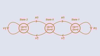
Some logic diagrams of that machine from my old design book for the graphics display.
Old design notes/scribbles on decodes and counters for this that I currently have only a faint memory of. The upper address lines were used as decode addresses and A15 was used as a master gate to switch to CPU control from TIMING control from the display address counters. The bank address decoder was a 74ls42 to access the boot rom, cpu memory, character generator memory, graphic memory, address counters for the video dot generator and I/O for the S100 bus. The INT pin was tied to a rs4020 14 bit counter that I think generated a video line based interrupt for the 8080. The memory was static 2114 (1k *4 bits) chips so no need for interrupts for that. Tri-state buffers connected to the bank address decoder separated data lines from the devices. Can't remember the exact resolution but the graphics frame buffer was only 2k *8bits, with a 1k 8080 GPU program ram and 1K character memory for the RO-3-2513 5*7 dot matrix chip.
I did the same thing with a Motorola MC6809 design.
Basically, you need a shift register that is continuously fed with data from SRAM that holds a bit map of your screen.
I guess I'm not that nostalgic for old technology having spent so much time keeping archaic systems running over the decades. It was cool building it long ago because it was somewhat current technology then.
The fun wasn't making a copy of a design, the fun was making your own design work using basic principles.
Some logic diagrams of that machine from my old design book for the graphics display.
Old design notes/scribbles on decodes and counters for this that I currently have only a faint memory of. The upper address lines were used as decode addresses and A15 was used as a master gate to switch to CPU control from TIMING control from the display address counters. The bank address decoder was a 74ls42 to access the boot rom, cpu memory, character generator memory, graphic memory, address counters for the video dot generator and I/O for the S100 bus. The INT pin was tied to a rs4020 14 bit counter that I think generated a video line based interrupt for the 8080. The memory was static 2114 (1k *4 bits) chips so no need for interrupts for that. Tri-state buffers connected to the bank address decoder separated data lines from the devices. Can't remember the exact resolution but the graphics frame buffer was only 2k *8bits, with a 1k 8080 GPU program ram and 1K character memory for the RO-3-2513 5*7 dot matrix chip.
I find the old technology interesting but I don't know it well enough to make my own designs yet so I figured copy others and learn more about it. Thanks for the diagrams! Is there a chance you have a higher resolution of them? When I zoom in they are quite fuzzy.
I did the same thing with a Motorola MC6809 design.
Basically, you need a shift register that is continuously fed with data from SRAM that holds a bit map of your screen.
I find the old technology interesting but I don't know it well enough to make my own designs yet so I figured copy others and learn more about it. Thanks for the diagrams! Is there a chance you have a higher resolution of them? When I zoom in they are quite fuzzy.
Those are just doodles that won't mean much unless you have most of the design in your head like I did back them. This was exploring some ideas about how to switch from CPU memory addressing (8080 boot PROM/SRAM banking) to graphic memory addressing from video counters or the GPU using tri-state buffers.
Those are just doodles that won't mean much unless you have most of the design in your head like I did back them. This was exploring some ideas about how to switch from CPU memory addressing (8080 boot PROM/SRAM banking) to graphic memory addressing from video counters or the GPU using tri-state buffers.
 Facebook
 Google
 GitHub
 Linkedin