Regular Diodes, Zener Diodes and BJT transistors

Thread Starter

Gersi266

Joined Dec 23, 2024
6
The assignment isn't in english but I will translate it for you.
Exercise 1:
Project a shunt regulator circuit with Zener. We're given the data Vz=20V, Izmin = 4mA. The source is 100V.
Find the value of R that allows the voltage to be adjusted from infinite RL to a minimum RL. What is the value of RL minimum?
Find the maximal possible value of the current for the charge in RL min
Draw the diode characteristics and show the point of work for each case.
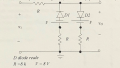
Exerise 2:
For the scheme shown in the figure, suppose that the diodes D1 and D2 are real.
a) Write the equations of the transfer characteristic (v0 as a function of vi), and graphically represent this characteristic by noting all the discontinuities, slopes, and voltage levels.
b)Graphically represent the output signal Vo(t) if the input signal Vi(t)=30sinwt acts.

Exercise 3:
For the 2-stage amplifier with BJT transistor shown in the figure, determine:
a) Current amplification AL, voltage amplification Av.
b) Voltage amplification taking into account the source resistance Avs.
c) Input resistance Ri and output resistance R0 of the amplifier at low frequencies.
d) Draw the shape of the output signal Vo(t) when Vi(t)=10sinwtEG57_ 2483.pngEG57_ 2484.png
 
Last edited by a moderator:

ericgibbs

Joined Jan 29, 2010
21,391
Hi G266.
Welcome to AAC.
As this a college assignment you need to post your best attempt at answering, then we can help.

Moderation.
 

Thread Starter

Gersi266

Joined Dec 23, 2024
6
Hi G266.
Welcome to AAC.
As this a college assignment you need to post your best attempt at answering, then we can help.

Moderation.
Hello Eric. Thank you for your response. I posted every information that we had to solve these question. Let me know what else might be needed and I’ll try to find that as well
 

Thread Starter

Gersi266

Joined Dec 23, 2024
6
Hi G,
I understand that you cannot solve the problem, but it is important to post how you tried to solve the problem, then we will then be able to offer assistance.

It is AAC's policy not to provide final solutions to homework or college work.
E

This link explains.
https://forum.allaboutcircuits.com/...ng-questions-in-the-homework-help-forum.3002/
I was able to solve only the first exercise.
When vi < 8V, both diodes are reverse-biased, and v0 = 0.
When vi > 8V, both diodes are forward-
biased. Applying KVL, we have:
Vi= vo + 2V + I
V0 = vi - 2V - I
Since the diodes are real, we need to consider the voltage drop across them.
Let's assume a constant voltage drop of
0.7V for simplicity. Then:
Vo = vi - 1.4V - I
If we assume the diodes are ideal, then
Vo =vi - 2V .
 

WBahn

Joined Mar 31, 2012
32,703
I was able to solve only the first exercise.
When vi < 8V, both diodes are reverse-biased, and v0 = 0.
When vi > 8V, both diodes are forward-
biased. Applying KVL, we have:
Vi= vo + 2V + I
V0 = vi - 2V - I
Since the diodes are real, we need to consider the voltage drop across them.
Let's assume a constant voltage drop of
0.7V for simplicity. Then:
Vo = vi - 1.4V - I
If we assume the diodes are ideal, then
Vo =vi - 2V .
The first exercise has just one diode -- a 20 V Zener diode. So your description makes no sense for that exercise.

It seems to apply to the second exercise, although it makes little sense and definitely doesn't come close answering the question that was asked.

How do you figure that both diodes are reverse-biased when Vi = -10 V?

How do you figure that both diodes are forward-biased when Vi = +10 V?
 

Thread Starter

Gersi266

Joined Dec 23, 2024
6
The first exercise has just one diode -- a 20 V Zener diode. So your description makes no sense for that exercise.

It seems to apply to the second exercise, although it makes little sense and definitely doesn't come close answering the question that was asked.

How do you figure that both diodes are reverse-biased when Vi = -10 V?

How do you figure that both diodes are forward-biased when Vi = +10 V?
I had uploaded the entire photo but it was edited by the moderators. The photos are only for exercise 2 and 3.
I noticed now that the exercise says the diodes are real so I have to take that into account as well.
For the first sentence of exercise 2:
Write the Equations of the Transfer Characteristic:
We have three cases:
Case 1: vi<−8−0.7V
Both D1 and D2 are reverse-biased because the input voltage vi is too low to forward-bias either diode.
The output voltage vo=vi because the circuit behaves like an open circuit.

Case 2: −8−0.7≤vi≤8+0.7

In this range:
D1 conducts when vi≥−8+0.7≈−7.3 
D2 conducts when vi≤8−0.7≈7.3 

Case 3: vi>8+0.7 V
Both D1 and D2 are reverse-biased.
The output voltage vo=vi again because the circuit behaves like an open circuit.
 

WBahn

Joined Mar 31, 2012
32,703
For the first sentence of exercise 2:
Write the Equations of the Transfer Characteristic:
We have three cases:
Case 1: vi<−8−0.7V
Both D1 and D2 are reverse-biased because the input voltage vi is too low to forward-bias either diode.
The output voltage vo=vi because the circuit behaves like an open circuit.
1734988564583.png

So let's pick vi = -10 V. You are claiming that vo = -10 V.

What are the voltages at points A, B, C, and D for this situation?

Are these voltages consistent with your assertion that both D1 and D2 are reverse-biased?
 

Thread Starter

Gersi266

Joined Dec 23, 2024
6
View attachment 338740

So let's pick vi = -10 V. You are claiming that vo = -10 V.

What are the voltages at points A, B, C, and D for this situation?

Are these voltages consistent with your assertion that both D1 and D2 are reverse-biased?
I think I figured out where my mistake is:

The circuit contains two diodes D1 and D2. For real diodes, we consider:

  • Forward voltage drop VD=0.7V
  • When forward biased: ID>0 when VD>0.7 V
  • When reverse biased: ID≈0
The transfer characteristic equation can be divided into three regions:

  1. When vi<0vi<0:
    • D1 is reverse biased
    • D2 is reverse biased
    • Therefore: vo=0
  2. When 0<vi<0.7V
    • D1 starts conducting
    • D2 is still reverse biased
    • Therefore: vo=vi
  3. When vi>0.7 V
    • D1 is conducting
    • D2 starts conducting
    • Therefore: vo=0.7 V (clamped at diode forward voltage)
The complete transfer characteristic equation is
1734989641419.png
Couldn't write it here so did it in a office document and screenshoted it. Am I correct until here?
 

WBahn

Joined Mar 31, 2012
32,703
Nope, that is not correct.

I'll ask again. If vi is -10 V, what are the voltages at the four labeled points in the diagram I provided?
 
Top