Facebook
 Google
 GitHub
 Linkedin
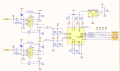
There is no requirement to use 30k, but some piece of information I read about suggesting using high input resistance for this type circuit so it was what I selected. If the OP AMP isn't required, I will look into redesigning it without it in the future.The net effect of the input circuit is a 30 K input impedance and a forward gain of 0.825. If the 30 K impedance is important (as in required by whatever is producing the input signal), then a 2-resistor attenuator followed by a simple voltage follower will produce the same low output impedance with fewer components, fewer error terms, and lower noise. And, you can cover both inputs with one dual opamp, eliminating U4.
Separate from that, why do the input circuit and A/D input have different grounds? Shouldn't the analog input conditioning stage be referenced to the same potential as the analog converter input? As it is now, any potential difference getween the two grounds, which mostly will be noise, will appear on top of the input signal at the A/D input.
ak
There are two separate grounds for digital and analog signals that meet toward the center of the board. This part of the design was difficult for me to solidify my understanding of what should be connected to which one, and it was an unintended mistake on my part that they reference two different grounds. It is fixed in the current edition of the board.
It isn't my idea or desire to use separate grounds in the first place, but I am a smaller part of a team of amatuers so a lot of this design is failing upward.