re; any help mppt

hgmjr

Joined Jan 28, 2005
9,027
then i am now looking at the output values to the DAC:
which reminds me, making a 10V reference, the digital outputs are 0 and 5V right?
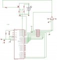
You don't need to worry about using 5V logic signals to control the DAC powered by 10V. The 5V digital IO lines are just being used to open and close digital switches in the DAC. These switches are used to select the taps in the R2R ladder network.

hgmjr
 

hgmjr

Joined Jan 28, 2005
9,027
oh, next is my connection of the the output from the microcontroller correct to the LSB and MSB of the DAC?
The schematic is not ultra clear. The best I can say is that the hook up between the DAC and the micro appear to be correct.

hgmjr
 

hgmjr

Joined Jan 28, 2005
9,027
ah yes i have seen the explanation of the negative value recieved and this is from the DAC - you can see from the datasheet, the 'table 1' for the analog output ;
Not sure which document you are referring to here.

hgmjr
 

hgmjr

Joined Jan 28, 2005
9,027
I think the outstanding questions you had have now been answered in posts 81 through 83.

I sent you the link to www.avrbeginners.net to help you get a better grip on the AVR interrupt handling.

I am about to begin another day at work so I will only be able check in a couple of times during the day.

Good luck with your efforts today.

hgmjr
 

Thread Starter

olusola

Joined May 21, 2007
74
below is the edited code to be able to get P0 the first power.

i'm hoping this should be ok,

how then do i reverse the output?


//***** First Conversion - Discard)
// Measure Voltage
ldi Temp, (1<<REFS1)|(1<<REFS0)|(0<<MUX0); set voltage meausurement channel and internal referece
out ADMUX, Temp;
sbi ADCSRA, ADSC; start A-D conversion

ADC_wait_K:; wait until A-D conversion finished
sbis ADCSRA, ADIF;
rjmp ADC_wait_K;

in Voltage_L, ADCL; Store Converted Low Bit value
in Voltage_H, ADCH; Store Converted High Bit value
//sbi ADCSRA, ADIF;

// Measure Current
ldi Temp, (1<<REFS1)|(1<<REFS0)|(1<<MUX0); set voltage meausurement channel and internal referece
out ADMUX, Temp;
sbi ADCSRA, ADSC; start A-D conversion

ADC_wait_C:; wait until A-D conversion finished
sbis ADCSRA, ADIF;
rjmp ADC_wait_C;

in Current_L, ADCL; Store Converted Low Bit value
in Current_H, ADCH; Store Converted High Bit value
//sbi ADCSRA, ADIF;

// Calculate Power Performing 10bit x 10bit = 24bit multiplication
// Power Calculated for first value to be used a start of climbing Algorithm

mul Voltage_H, Current_H; AH*BH
mov Power_Old_H, Mul_L;
mul Voltage_L, Current_L; AL*BL
mov Power_Old_M, Mul_H;
mov Power_Old_L, Mul_L;
mul Voltage_H, Current_L; AH*BL
add Power_Old_H, Mul_H;
add Power_Old_M, Mul_L;
mul Current_H, Voltage_L; BH*AL
add Power_Old_H, Mul_H;
add Power_Old_M, Mul_L;


sei; // Enable Global Interrupts...

// Idle in this "do-nothing" loop waiting for next interrupt....

Loop_here:
rjmp Loop_here
 

hgmjr

Joined Jan 28, 2005
9,027
below is the edited code to be able to get P0 the first power.

i'm hoping this should be ok,

how then do i reverse the output?
By "reverse the output" do you mean invert the output of the DAC?

Rich (BB code):
//***** First Conversion - Discard)
// Measure Voltage ( This read is the one you planned to discard)
ldi Temp, (1<<REFS1)|(1<<REFS0)|(0<<MUX0); set voltage meausurement channel and internal referece
out ADMUX, Temp;
sbi ADCSRA, ADSC; start A-D conversion
 
ADC_wait_K:; wait until A-D conversion finished 
sbis ADCSRA, ADIF;
rjmp ADC_wait_K;
 
in Voltage_L, ADCL; Store Converted Low Bit value
in Voltage_H, ADCH; Store Converted High Bit value
//sbi ADCSRA, ADIF;
 
// Measure Voltage    (This one is for real....)
ldi Temp, (1<<REFS1)|(1<<REFS0)|(0<<MUX0); set voltage meausurement channel and internal referece
out ADMUX, Temp;
sbi ADCSRA, ADSC; start A-D conversion
 
ADC_wait_K:; wait until A-D conversion finished 
sbis ADCSRA, ADIF;
rjmp ADC_wait_K;
 
in Voltage_L, ADCL; Store Converted Low Bit value
in Voltage_H, ADCH; Store Converted High Bit value
 
// Measure Current
ldi Temp, (1<<REFS1)|(1<<REFS0)|(1<<MUX0); set voltage meausurement channel and internal referece
out ADMUX, Temp;
sbi ADCSRA, ADSC; start A-D conversion
 
ADC_wait_C:; wait until A-D conversion finished 
sbis ADCSRA, ADIF;
rjmp ADC_wait_C;
 
in Current_L, ADCL; Store Converted Low Bit value
in Current_H, ADCH; Store Converted High Bit value
//sbi ADCSRA, ADIF;
I have added a suggested code change.
 

hgmjr

Joined Jan 28, 2005
9,027
I don't suppose you have had a chance to update the schematic. Once you have it cleaned up a bit, it would be a good idea to post a fresh one.

hgmjr
 

hgmjr

Joined Jan 28, 2005
9,027
I have reviewed the new schematic and it is pretty much in reasonable shape.

A couple of things to consider.

1. At the DAC, you will need to connect the Vref pin to +10 volts instead of +15V since your positive supply voltage to the DAC is 10V.

2. You can power the opamp with +/-10V instead of instead of +/-15V. Under normal control operation conditions the output of the opamp should not need to go more positive that 7.5V. In fact you may want to consider powering the opamp from +10 and ground. I don't think the negative 10V is going to buy you anything. Remember the mosfet's gate will only need to swing from a minimum of 1 volt to a maximum of around 7.5 volts (this factors in the voltage drop across the 1.25 ohm resistor) to turn the mosfet from completely off to completely on.

If you have no questions on my hardware comments above then we can continue looking at the software.

hgmjr
 

hgmjr

Joined Jan 28, 2005
9,027
Have I answered all of your software questions up to now or are there still some nagging questions.

Your flow-chart will need to change a bit to reflect the newly added idle loop. To make it clear you will need to flowchart the interrupt service routine as a subroutine separate from the main code execution section. I will try to sketch a suggested modification for you to consider.

hgmjr
 

Thread Starter

olusola

Joined May 21, 2007
74
I have reviewed the new schematic and it is pretty much in reasonable shape.

A couple of things to consider.

1. At the DAC, you will need to connect the Vref pin to +10 volts instead of +15V since your positive supply voltage to the DAC is 10V.

hgmjr
the DAC positive supply as in the diagram is +15V and the Vref is 10V . should i change it?


2. You can power the opamp with +/-10V instead of instead of +/-15V. Under normal control operation conditions the output of the opamp should not need to go more positive that 7.5V. In fact you may want to consider powering the opamp from +10 and ground. I don't think the negative 10V is going to buy you anything. Remember the mosfet's gate will only need to swing from a minimum of 1 volt to a maximum of around 7.5 volts (this factors in the voltage drop across the 1.25 ohm resistor) to turn the mosfet from completely off to completely on.
ok, this is just to change the power supply, as for now i'm using variable power supplies.

thanks
 

hgmjr

Joined Jan 28, 2005
9,027
Yes. Go ahead and connect +10V to the Vref pin and the V+ pin of the DAC. In you application these two pins can and should be the same voltage.
 

Thread Starter

olusola

Joined May 21, 2007
74
can i ask where you got the information about the voltages for the mosfet from 1V to 7.5V?
also any ideas or how can i estimate the swing of resistance (drain-source?) for these values?

thanks
 

Thread Starter

olusola

Joined May 21, 2007
74
HI,
how do you suggest i run this algorithm?
is the current one in the program ok?

what section of it do you think i need to work more on?

how then do i calibrate this- as in for the software how do i respond to this voltage changes.

also how do i reverse the output so it comes out positive after the DAC?

thanks
 

hgmjr

Joined Jan 28, 2005
9,027
can i ask where you got the information about the voltages for the mosfet from 1V to 7.5V?
A mixture of 80% manufacturer's datasheet and 20% experience.

The manufacturer's datasheet (at least the one I pulled up) indicated that the maximum Vgs (voltage between the gate and source terminals) required to turn the mosfet completely on is 5V. You stated in an earlier email that you expected a maximum solar panel current of 2 Amps. Ohms law says that a 1.25 ohm resistor with 2A flowing through it will have a voltage dropped across it of 1.25 V times 2A which comes to 2.5V. That means that when the active load is dumping 2A, the source terminal of the mosfet will be at a potential of 2.5V more positive than ground (0V). 5V plus 2.5V is equal to 7.5. This is a rough calculation mind you but close enough for the purpose of this design.

also any ideas or how can i estimate the swing of resistance (drain-source?) for these values?

thanks
That is a bit more involved since it requires using the graphs in the manufacturer's datasheet and probably the use of load line analysis to estimate these operating points.

The fact that the control signal to the mosfet is in the feedback loop means that only the minimum and maximum values of the range need to determined to insure that your control signal source swings fully over this range.

Is it critcal for you to know this information? If so, I will try to see if I can come up with something.

hgmjr
 

Thread Starter

olusola

Joined May 21, 2007
74
also any ideas or how can i estimate the swing of resistance (drain-source?) for these values?

thanks

That is a bit more involved since it requires using the graphs in the manufacturer's datasheet and probably the use of load line analysis to estimate these operating points.

The fact that the control signal to the mosfet is in the feedback loop means that only the minimum and maximum values of the range need to determined to insure that your control signal source swings fully over this range.

Is it critcal for you to know this information? If so, I will try to see if I can come up with something.
oh ok, it is not required then . well at least not yet.


2. Now i really am not sure about the algorithm in the code.
do you think with what is written it will cope with the range or is there a need to like -calibrate it?

thanks
 

hgmjr

Joined Jan 28, 2005
9,027
HI,
how do you suggest i run this algorithm?
Do you mean how so you test the algorithm?

is the current one in the program ok?
There a few things that need attention but the framework seems workable.

what section of it do you think i need to work more on?
I need to look at that a little more and then get back with you shortly.

how then do i calibrate this- as in for the software how do i respond to this voltage changes.
Not clear on what you mean by calibrate in the above question.

also how do i reverse the output so it comes out positive after the DAC?

thanks
That is the easiest thing of all. In your flowchart you indicate that when P1 > P0 you increment the value you output to the DAC. Incrementing the binary value fed to the DAC will result in an increase in the voltage applied to the mosfet gate. As I indicated, when the voltage increases on the gate more current is drawn from the solar panel by the mosfet active load. If this is consistent with what you want the active load to do then no change to your program logic is required. If not, then all you need to do is change the action from increment to decrement and you are good to go. This is how you invert the sense of the control.

hgmjr
 
Top