Push pull drive question

Thread Starter

Aleph(0)

Joined Mar 14, 2015
597
Just so you know this is NOT an Ltspice question:cool:

So HP gave me schematic of Royer oscillator as test circuit for rebuilt LOPT transformers (which are just old TV flyback transformers optimized for HV power supplies). Anyhow the circuit works perfectly but I don't totally understand base drive so I can't use it for instructional material in good conscience until point of confusion is cleared up and HP is too busy for me to dare bug her with any of this until next week:(

So b4 I state question plz let me say this:
L6 is feedback winding
L7 & L5 are tapped primary winding
L8 is HV secondary

So here's problem that I just can't understand:(!
It looks to me like the negative end of feedback winding (L6) will be floating cuz B-E junction of BJT at negative end of L6 will be reverse biased? So how can positive end of L6 drive any current to bias its BJT?

To understand what I'm saying plz just think on this:

Say end of L6 on Q3 is positive (more than 0v with respect to ground and emitter of Q3) and also above silicon forward bias threshold (like 0.6v). So in order to supply bias current to Q3 base, other end of L6 needs ground reference but it's floating cuz it's negative which reverse biases b-e junction of Q4:confused:

Also putting external fast diodes across b-e junctions (with cathode to base and anode to ground) to give negative signal a ground reference seriously F's the performance of the circuit:confused:!

So I know I'm being stupid somewhere cuz it works great as drawn in real life and on simulator but I just don't get it and curiosity and need to move past it is stronger than pride at this point:)

Thanks an advance!


MyRoyer.jpg
 

MrAl

Joined Jun 17, 2014
11,464
Hello there,

You sure there is no second 1k resistor from the positive input to the base of Q4? That would be more typical i think.

Anyway, Q4 will start to turn off through a lack of Beta and once that winding becomes positive on top that will help Q4 turn off faster, and once Q3 starts to turn off via same physical characteristic the bottom of that winding becomes a little more positive so should turn on Q4 faster.

We could be more sure of everything if you post your .asc file and i'll run it myself, or you could study the base signals yourself if you like.

You might also define how you determine how a circuit like this is deemed to "work", as it may do better with an improvement and may only appear to work as well as it should be working. For example, Q3 may get hotter than it needs to until an improvement is made A careful simulation analysis would tell us more.
 
Last edited:

Thread Starter

Aleph(0)

Joined Mar 14, 2015
597
You sure there is no second 1k resistor from the positive input to the base of Q4? That would be more typical i think.
No it's just pulled up at one end cuz bias voltage is DC (so XL doesn't matter) and winding is just 2 to 3 turns of 18 AWG so insignificant resistance:)

Anyway, Q4 will start to turn off through a lack of Beta and once that winding becomes positive on top that will help Q4 turn off faster, and once Q3 starts to turn off via same physical characteristic the bottom of that winding becomes a little more positive so should turn on Q4 faster.
But what I'm not understanding is how can the positive end can drive current into the base it's connected to when the other end (which has to be negative cuz winding is not electric monopole;)) is just floating cuz of negative biasing of the b-e junction it's connected to:confused:?

We could be more sure of everything if you post your .asc file and i'll run it myself, or you could study the base signals yourself if you like.
Ok it (should) be attached to this post THANKS:)!
 

Attachments

Thread Starter

Aleph(0)

Joined Mar 14, 2015
597
you could study the base signals yourself if you like.
According to simulator base signal is just waveform spanning from silicon bias threshold to ≈ 0-(input supply voltage) so if that means circuit only works by breaking down b-e junction on 'off' transistor I'm finding it hard to believe cuz circuit keeps working w/o degrading performance:confused:
 

#12

Joined Nov 30, 2010
18,224
breaking down b-e junction on 'off' transistor I'm finding it hard to believe cuz circuit keeps working w/o degrading performance:confused:
Reversing the current in a B-E junction does not poison it if the current is within acceptable limits, like power dissipation limit. Be aware that a reverse current will show up as about 5v to 7 v reverse voltage.
 
Last edited:

OBW0549

Joined Mar 2, 2015
3,566
I'm no expert on these Royer oscillator circuits, but the way I see it base drive current to turn on Q3/Q4 is provided by R2, and L6 merely turns off whichever transistor is supposed to turn off. Adding base diodes, as you tried, probably ends up overdriving the ON transistor, which increases its turn-off time and thus garfs everything up, as you observed.
 

MrAl

Joined Jun 17, 2014
11,464
According to simulator base signal is just waveform spanning from silicon bias threshold to ≈ 0-(input supply voltage) so if that means circuit only works by breaking down b-e junction on 'off' transistor I'm finding it hard to believe cuz circuit keeps working w/o degrading performance:confused:
Hi again,

Well, you are claiming that it does not degrade performance (ie "works") but did you study the workings well enough to make that kind of statement and be sure it is completely correct? I ask about this in a nice way, but in light of your previous claim of not believing that it could work at all has me wondering if you should be making a claim which requires an even more in depth study of the circuit (which is one point i was making in my previous post). In short, you seem to be saying, "i dont know how this circuit works in full, but i know it is working as well as it ever can be working". In my opinion you know it pretty well though anyway.

So take a look at OBW's post, and see if that makes sense to you first. As the winding current seeks one base emitter low resistance, it finds the other one of higher impedance. That might help answer your main question.

But as to the circuit working "without degrading performance" i might want to look into. One reason is because the bias will not be symmetrical, with with a non symmetrical transistor drive we have somewhat non symmetrical saturation characteristics, and with that we probably have a non symmetrical transformer primary drive, and with a non symmetrical transformer drive we have non symmetrical primary currents, and with non symmetrical primary currents we have DC offset in the primary which means more loss in the primary and/or the DC choke in series with the center tap. Just a gut feeling but this should be investigated as well as any other non symmetrical drive problems such as increased overlap of transistor 'on' times. Cant hurt to look into this.

Now that we have the .asc file we can all do some simulations. I'll try to do some tomorrow some time if not sooner.
You know you can always try it both ways, with 1k and with 1M resistors on that second transistor base ... see what you can find out. Look for any differences especially improvements.
 

crutschow

Joined Mar 14, 2008
34,412
I'm no expert on these Royer oscillator circuits, but the way I see it base drive current to turn on Q3/Q4 is provided by R2, and L6 merely turns off whichever transistor is supposed to turn off. ..................
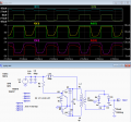
According to the simulation below, you are correct.
L6 is rather acting like a switch.
When the top side of L6 is positive, no current is flowing through L6 (thus no reverse Q4 base current) and the R2 resistor current is flowing into Q3's base.
When the bottom side of L6 is positive, the resistor current is flowing through L6 into Q4's base, and Q3's base is reverse biased.

upload_2016-11-16_0-32-23.png
 

DickCappels

Joined Aug 21, 2008
10,169
I have designed a few CRT deflection and high voltage power supplies and OBW0549's explanation rings true.

In one paper an engineer with Motorola Semiconductor wrote that it is preferred to avalanche the emitter-base junction with as much current as was going into the base just prior to initiation of turn-off in order to speed up turnoff, thus reducing turn-off losses. The only degredation observed was a decrease in low current beta (so nobody cares), and this is in agreement with #12's observation in post #5.
 
According to the simulation below, you are correct.
L6 is rather acting like a switch.
When the top side of L6 is positive, no current is flowing through L6 (thus no reverse Q4 base current) and the R2 resistor current is flowing into Q3's base.
When the bottom side of L6 is positive, the resistor current is flowing through L6 into Q4's base, and Q3's base is reverse biased.

View attachment 115402
Given the way the low voltage driven windings are placed on the leg of the core away from the high voltage tire (this is not Aleph(0)'s actual setup and I show it only to remind us where the low voltage windings are placed):

http://forum.allaboutcircuits.com/attachments/testkludge-jpg.89686/

it's unlikely that the coefficient of coupling between L8 and the other windings is anywhere near unity. The coupling coefficient between the other windings is not unity either, and the concomitant leakage inductance may have a noticeable effect on circuit performance.
 

Thread Starter

Aleph(0)

Joined Mar 14, 2015
597
Reversing the current in a B-E junction does not poison it if the current is within acceptable limits
#12 that makes sense cuz I remember way back in oo's restoring clunky old hf xcvr (iirc hw101) which used reverse biased b-e jct of to92 bjt for zener in its vfoo_O! I totally forgot that until you said it:oops:!

I'm no expert on these Royer oscillator circuits, but the way I see it base drive current to turn on Q3/Q4 is provided by R2, and L6 merely turns off whichever transistor is supposed to turn off. Adding base diodes, as you tried, probably ends up

overdriving the ON transistor, which increases its turn-off time and thus garfs everything up, as you observed.
OBW0549 TNX! Cuz I wasn't even thinking on that perspective:oops: So that means the bias resistor provides the _ground reference_ through the LV power supply:)? Got it:cool:!

Well, you are claiming that it does not degrade performance (ie "works") but did you study the workings well enough to make that kind of statement and be sure it is completely correct? I ask about this in a nice way, but in light of your previous claim of not believing that it could work at all has me wondering if you should be making a claim which requires an even more in depth study of the circuit (which is one point i was making in my previous post). In short, you seem to be saying, "i dont know how this circuit works in full, but i know it is working as well as it ever can be working". In my opinion you know it pretty well though anyway.
MrAl I'm sry if I wasn't clear I just meant I can run the circuit for hours and when I recharacterize the bjts on my b1500a there's no statistically significant changes from preprototype characterization so I'm just saying whatever's happening it's not altering the transistors:) So I admit I'm clueless about circuit except to say that it does what HP claims and doesn't eat the bjts:cool:!

but this should be investigated as well as any other non symmetrical drive problems such as increased overlap of transistor 'on' times. Cant hurt to look into this.
MrAl that's a good point to look in to all that so we're not pushing core like saturable reactor:eek:! Just so you know, purpose of choke apart from PSU decoupling is reactive buffer for overlapping conduction angle of bjts:)

According to the simulation below, you are correct.
L6 is rather acting like a switch.
When the top side of L6 is positive, no current is flowing through L6 (thus no reverse Q4 base current) and the R2 resistor current is flowing into Q3's base.
When the bottom side of L6 is positive, the resistor current is flowing through L6 into Q4's base, and Q3's base is reverse biased.
Crutschow tnx for walking through that for me:)! When I looked at base voltage with Ltspice all I saw was like envelope of 39khz pulses which started as a line at like +0.7v (cuz of silicon bias voltage?) which expanded downward more or less linearly over period of abt 34uS until max negative peaks were at abt -40V:confused::oops: So I'm saying thanks cuz your plots are a lot more useful for understanding circuit:)!

In one paper an engineer with Motorola Semiconductor wrote that it is preferred to avalanche the emitter-base junction with as much current as was going into the base just prior to initiation of turn-off in order to speed up turnoff, thus reducing turn-off losses. The only degredation observed was a decrease in low current beta (so nobody cares), and this is in agreement with #12's observation in post #5.
DickCappels Tnx! So if I'm understanding right it's a combination of the nondestructive avalanching of the junctions and the observations of OBW0549 and Crutschow that make the circuit work in real world but just the observations of OBW0549 and Crutschow that make it simulate correctly (cuz ltspice doesn't support avalanching of BJT junctions)?

Given the way the low voltage driven windings are placed on the leg of the core away from the high voltage tire
http://forum.allaboutcircuits.com/attachments/testkludge-jpg.89686/
Electrician Tnx! Cuz that's how the transformer is setup with the HV winding on one leg and the coaxially wound primary and feedback windings on the other:)

this is not Aleph(0)'s actual setup and I show it only to remind us where the low voltage windings are placed
Right cuz we have a totally better driver the one in the pic is just embarrassing:eek::oops:

it's unlikely that the coefficient of coupling between L8 and the other windings is anywhere near unity. The coupling coefficient between the other windings is not unity either, and the concomitant leakage inductance may have a noticeable effect on circuit performance.
You'll have to ask HP abt particulars but iirc unity coupling was chosen just to make ltspice happy cuz you're right there's got to be major leakage inductance with airgapped ferrite core:cool:!
 
Last edited:
So that means the bias resistor provides the _ground reference_ through the LV power supply:)? Got it:cool:!
Aleph!:rolleyes: Please carefully read @OBW0549 's reply! -- He's stating that current from V1 (via R2) forward biases the B-E junction of either Q3 or Q4 dependent upon the induced 'electrical state' of L6 --- An analysis with which, BTW, I wholeheartedly agree:)

@crutschow -- I wish to add my thanks for your LtSpice presentation! -- It's taught me a 'new' simulator technique:):):)

See Y'all next week
HP:)
 
Last edited:
@Aleph(0)

Here's an experiment for you:

Physically connect the circuit as shown in post #1 but with the following changes:

1) Remove R2.
2) Tie the base of Q3 to the V1 rail with a 2.2 kΩ resistor.
3) Tie the base of Q4 to the V1 rail with a 2.2 kΩ resistor.
4) Account for circuit behavior and reconcile same with LtSpice.
5) Repeat 2, 3 and 4 above but with 1kΩ and 470Ω resistors...


Have fun!
HP:)
 
Last edited:

MrAl

Joined Jun 17, 2014
11,464
#12 that makes sense cuz I remember way back in oo's restoring clunky old hf xcvr (iirc hw101) which used reverse biased b-e jct of to92 bjt for zener in its vfoo_O! I totally forgot that until you said it:oops:!


OBW0549 TNX! Cuz I wasn't even thinking on that perspective:oops: So that means the bias resistor provides the _ground reference_ through the LV power supply:)? Got it:cool:!


MrAl I'm sry if I wasn't clear I just meant I can run the circuit for hours and when I recharacterize the bjts on my b1500a there's no statistically significant changes from preprototype characterization so I'm just saying whatever's happening it's not altering the transistors:) So I admit I'm clueless about circuit except to say that it does what HP claims and doesn't eat the bjts:cool:!


MrAl that's a good point to look in to all that so we're not pushing core like saturable reactor:eek:! Just so you know, purpose of choke apart from PSU decoupling is reactive buffer for overlapping conduction angle of bjts:)


Crutschow tnx for walking through that for me:)! When I looked at base voltage with Ltspice all I saw was like envelope of 39khz pulses which started as a line at like +0.7v (cuz of silicon bias voltage?) which expanded downward more or less linearly over period of abt 34uS until max negative peaks were at abt -40V:confused::oops: So I'm saying thanks cuz your plots are a lot more useful for understanding circuit:)!


DickCappels Tnx! So if I'm understanding right it's a combination of the nondestructive avalanching of the junctions and the observations of OBW0549 and Crutschow that make the circuit work in real world but just the observations of OBW0549 and Crutschow that make it simulate correctly (cuz ltspice doesn't support avalanching of BJT junctions)?


Electrician Tnx! Cuz that's how the transformer is setup with the HV winding on one leg and the coaxially wound primary and feedback windings on the other:)


Right cuz we have a totally better driver the one in the pic is just embarrassing:eek::oops:


You'll have to ask HP abt particulars but iirc unity coupling was chosen just to make ltspice happy cuz you're right there's got to be major leakage inductance with airgapped ferrite core:cool:!

Hi again,

Are you saying that you have one actually bread boarded and up and running? That makes this that much more interesting :)
Last time i had to deal with a physical Royer was back in the early 1980's when we used one for converting a solar array DC voltage into four or more isolated DC voltages for running the 100 amp transistor H bridge bias voltages for converting the array DC into 120vac line voltage for a line tied application. That's a long time ago so i cant remember everything. But if you have one running now you can check it for various things if you have a scope.

In the real life unit you can check the efficiency of course, which will tell all.
You can check for one transistor getting hotter than the other.

In the simulation we could check for DC offset, but we need a lot longer run time in the simulation (Carl you might want to try this). The longer run time will show the DC ratcheting if the non symmetricalness because of the base drives is too bad.

Just some ideas :)

BTW i always hated these circuits a little bit. That's mostly because they never had any built in dead time and need a separate choke to keep high currents down (BTW that only limits the DC ratchet current if the ESR of the choke is high enough even though it protects the transistors from high peak currents during the switchover transition period).
 

MrAl

Joined Jun 17, 2014
11,464
Hi again,

Am i seeing this circuit right? If so, some major problems.

First, if the output is 50kv and the load 100megs the output current is around 500ua and with a turns ratio of around 600 that means about 0.3 amps on the primary. However, with 1N914 (or equivalent) diodes on the output the current is going to be MUCH higher because the diodes will conduct too much in reverse mode as they are only rated for around 75 volts reverse. That will skew all results beyond reason.

So the first thing to do is get rid of those diodes and either replace them or change the rating or just use a resistive load and look at the AC output instead of the DC output for now. That's no rectification, but that wont hurt for initial tests of the converter section itself.

Second, the reverse voltages being applied to the base of the transistors is wayyy too high. I'm seeing like -40v which is way too high for most transistors. That will blow out any real transistor. I havent looked at the effect it has on the simulated transistors yet though.

Third, you should also check the rating on the Schottky diodes. I did not have the models for the ones you put in your circuit so i had to switch to something else. The voltage rating has to be high enough though to handle the primary peak voltages. I used 100v diodes instead.

The problem with diodes with voltage ratings too low is that they will draw rather large currents in the reverse direction which is completely unacceptable and will render any results from the simulation moot :)

Lastly, this is looking like a type of resonant converter rather than a simple switch mode where we see squarish waveforms and that happens because of that capacitor most likely and the inductances in the circuit. So we may see sinusoidal or half sinusoidal looking wave shapes once all the problems are fixed.

Should be interesting :)
 

OBW0549

Joined Mar 2, 2015
3,566
OBW0549 TNX! Cuz I wasn't even thinking on that perspective:oops: So that means the bias resistor provides the _ground reference_ through the LV power supply:)? Got it:cool:!
I'm not sure what you mean by "provides the ground reference"; current (approx. 30 mA) flows from V1 down through R2 to the bases of Q3 and (through L6, which has essentially zero resistance) Q4. Were there no feedback via inductive coupling, both transistors would be ON (at least to the extent that their Vbe's are matched) and the voltage at their bases would be approximately +0.7 volts. However, because of the feedback, the voltage induced in L6 will depress the voltage on one of the bases below Vbe(on), turning that transistor off. Providing the phasing is correct, this will result in sustained oscillations because of the resonance of C2 and L7.

I'm not sure to what degree L6 provides any turn-on drive current to the transistors beyond what flows down through R2; there may be some, but I don't think adding base drive is the dominant effect here.
 

#12

Joined Nov 30, 2010
18,224
the reverse voltages being applied to the base of the transistors is wayyy too high. I'm seeing like -40v
Reversed B-E junctions will not support -40V. They break over around -5v to -7v. Therefore, I think this is a simulation artifact.

Bordodynov is generally a brilliant designer, but his addition of B-E diodes is contrary to using reverse current to decrease switching time to the "off" condition as described by DickCappels. I didn't say this is good or bad, I just said that's how it's going to work.
 
Top