Facebook
 Google
 GitHub
 Linkedin
Hello,I have created a circuit as shown below based on a tottaly wrong circuit i was given.LTSPICE file is attached.
My circuit created a delay from M12 and P12.
This circuit is supposed to bias the gate of TGA2227 with -2.5V.
So i ahve -12V and i can create out of it -2,5V is many ways.
I could do voltage divider, I can use LM337 regulator.
What is the logic in using opamp and then resistor and zener diode to create -2.5V on the gate?
(The schematics is wrong, i just need to understand the logic)
Thanks.
https://www.qorvo.com/products/p/TGA2227-SM#documents
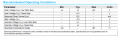
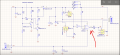

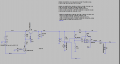
My circuit created a delay from M12 and P12.
This circuit is supposed to bias the gate of TGA2227 with -2.5V.
So i ahve -12V and i can create out of it -2,5V is many ways.
I could do voltage divider, I can use LM337 regulator.
What is the logic in using opamp and then resistor and zener diode to create -2.5V on the gate?
(The schematics is wrong, i just need to understand the logic)
Thanks.
https://www.qorvo.com/products/p/TGA2227-SM#documents
Attachments
-
4.9 KB Views: 1
Last edited: