Project: Photographic methods of making PCBs

Thread Starter

Lestraveled

Joined May 19, 2014
1,946
First, I would like to pay homage to Wendy Marsden and her contribution of her thread on making PCBs with the toner transfer method. It is a lot of work to put together a thread like that. In that thread, she said she would like to see someone start a thread on the photographic method of making PCBs and thus, I was motivated to create this tread. Thank you Wendy.

This thread is about making PCBs using photographic processes beginning with transparencies (artwork) produced from a laser or inkjet printer. There is a lot of flexibility when you choose the photographic path. So, this thread is not about one way of making PCBs photographically, it is about all the ways to make PCBs photographically. Based on your set of conditions and preferences, there are a variety of tools and options that you can use to optimize your PCB fabrication. Each process has its benefits and its costs.

Many of us in this community have a lot of experience making our own PCBs and we have our own ways of how to do it. I think it would be truly interesting and beneficial to hear about how the other guy makes their boards and especially, why they do it that way. I know that I have wrestled with making PCBs for a long time, and some of those times, the PCB has won.

So, I will start by presenting how I make PCBs and why I do it that way. Afterwards, I will take each function and expand on it, so that you can, if you want to, use it in your PCB fabrication.
 
Last edited:

Thread Starter

Lestraveled

Joined May 19, 2014
1,946
The process outlined below is the result of years of messing up a lot of PCBs. Frustration and wasting money are great motivators for me. As a result I have honed my process down to the essentials that guarantee me that when I finish, at least 90% of the PCBs I make are in the excellent category, and that I have not spent a lot of money doing it. I get no satisfaction from working several hours, burning through some money and then coming out of the shop with a handful of ratty looking PCBs. So, if a step, like turning my artwork into litho film, will significantly improve the quality and yield, I will spend the extra time and effort to insure that I am happy with the fruits of my labor.

Even though I have used a lot of them, I am not a fan of pre-sensitized positive PCBs. I think they are too expensive and too inconsistent. Also, you cannot tell if the exposure was correct until you put it in the etchant. At that point, if the exposure was not correct, then the board is not reusable. I hate wasting money. I am sure that I have messed up enough pre-sensitized positive boards to pay for the laminator that I now use to apply negative resist film to PCB stock. At minimum, this topic should inspire a lively discussion.

Outline of my process (Details of all of the processes are in later posts)

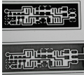
I print 3 or 4 positives of the PCB image on laser transparency film. (My laser printer does not print very dark.) I then stack/align them together to increase the density of the black image. The following pictures are of a single transparency and of 4 transparencies aligned.

Single transparency


Four Transparencies aligned on top of one another


I then use Litho film to reverse the image and to increase the contrast. The benefits of using Litho film, as well as how to use it, are covered in a later post.


Once the artwork is ready, it is time to sensitize the PCB stock. I use negative acting dry film resist. This film is a photo sensitive emulsion sandwiched between two protective sheets of plastic. One side of the plastic is removed and a laminator is used to apply it to the PCB stock. Dry Film resist has proven itself to be more reliable and precise than pre-sensitized positive PCB stock, plus it is much much cheaper. Again, this is covered in detail, with a video, in a later post.


It is now time to expose the PCB. I use a contact print frame to hold everything together while exposing. I use a 5 watt UV LED (365nm) as my light source. Once exposed, the image is clearly visible on the PCB. This is a nice feature of dry film resist. If there is a problem, the board can be stripped and re-laminated in just a few minutes.


The second layer of plastic strips off easily and the board is developed in a solution of Sodium Carbonate and water.


Development complete


I etch my boards in Sodium Persulfate using an economy etcher. Using this etcher has greatly reduced my consumption of sodium persulfate. I can etch three times the number of boards for the same amount of sodium persulfate as compared to using an unheated tray. It is a lot faster also.


The finished board (on a light box)


While the above process might seem a bit advanced for a home hobbyist, it works very well and is very reliable. If you are making more than one board, then it works even better. Good artwork is the key to success regardless of the photo resist you are using. You may not be interested in going through all of the above steps, but I am certain that you will find something of value in this thread that will improve the success rate, and or reduce the cost, of your PCB process.

There are videos in later posts that detail all of the above actions.
 
Last edited:

Thread Starter

Lestraveled

Joined May 19, 2014
1,946
Laser transparencies – What you see is not what you get – Something you need to know

This applies to both positive and negative acting resists

My HP1160 laser printer does not print very dark on transparencies. I have set the print density to 5, econo mode to off, and tried HP and aftermarket cartridges. A grainy dark gray is as dense as it gets, so I have to print 3 or 4 transparencies and align them on top of one another (stack up) to get the density/contrast up. Then I use the stack up as the master for the litho film. In the next picture there is a positive litho film on the left and the stack up on the right.


They both look very good....... in visible light, but PCB resist does not expose in visible light, it responds to a narrow band of UV light. In other words, what you see in visible light, is not what you get in ultra violet light. A significant factor is that plastic attenuates UV light a lot. Every plastic transparency I add to improve the density of the black image, reduces the transparency of the clear image at ultra violet. With every layer of plastic I add, the entire artwork gets darker at UV and contrast is lost. This throws off the exposure times and shrinks the optimal exposure time window (the sweet spot).

It is a little difficult to demonstrate this effect. We cannot see 365nm wavelength UV light and I don’t have UV light meter. We can demonstrate this indirectly by observing how much a piece of white paper fluoresces due to the UV light striking it.

The following picture needs some explanation. On the bench is a white sheet of paper lying flat. 12 inches above the paper, is an ultra violet light source (365nm) shining down. There is a plastic box on opposite sides of the paper. On top of each box is a transparency that extends over the paper. The two transparencies are arranged so that they cast a shadow on the paper. The art work on the left is a single layer litho film. The art work of the right is four layers of laser transparency film. The same PCB image is on both films.


Notice the shadow of the litho film on the left. It is bright and has high contrast. Compare it to the shadow on the right. The shadow on the right has reduced intensity and reduced contrast. This is due to it having four layers of plastic. These two pieces of artwork looked almost identical in visible light, and as you can see, they are very different at Ultra Violet. The reduced intensity directly impacts your exposure time. The reduced contrast shrinks the time difference between a board being under exposed and over exposed.

Bottom line: If your laser printer prints a very dark dense image and you only need one or two layers of transparencies to get good density, then you probably can safely bypass using Litho film. If your laser printer is crappy, like mine, then consider adding a litho film step in your process. You will not regret it. Turning my artwork into litho film has had a huge impact on the quality and yield of my PCB making.
 
Last edited:

Thread Starter

Lestraveled

Joined May 19, 2014
1,946
Artwork and exposing

This applies to both positive and negative acting resists

The art work is the photographic pattern used to control where the copper is going to remain on the PCB stock. With positive artwork, the image is black where the copper will stay, and with negative artwork, the image is clear where the copper will stay. The pattern is transferred to the sensitized PCB by a process called “contact printing”. The artwork is laid directly on top of the sensitized PCB, and a UV light source shines through the artwork and on to the photo resist. With positive resist, the exposed areas soften and will be washed away when developed. With negative resist, the exposed areas will harden and remain when developed.

During the exposure, the artwork must be pressed firmly against the surface of the PCB. This is normally done with a “contact printing frame (or easel)”. The construction of a printing frame is fairly simple. From the bottom up, you start with a flat solid base such as Plywood, MDF, ¼” glass etc. (Flatness is very important.) Next is a sheet of foam rubber, ¼” is good. Next is your sensitized PCB, resist side up. Next is the artwork. Then finally a sheet of glass, ¼” is good. Binding clips, rubber bands, or spring clips hold the “sandwich” together. The sandwich is then placed under the UV light source and exposed. You can also purchase a photographic contact printing frame.


You will see the above printing frame in use in later videos.

Off Contact Exposure
There is a condition called “off contact exposure”. This is when there is a gap between the artwork and the PCB resist (off contact) and the exposing light undercuts the artwork pattern. This can result in cut traces when positive resist is used and shorted traces when negative resist is used. Off contact exposure is caused by several things; not enough pressure on the “sandwich”, a warped PCB or base. A major cause of off contact exposure is wrinkles in the artwork, especially if layered laser transparencies are used. A laser printer uses heat to melt the toner on to the plastic transparency. This heat distorts the plastic transparency, thus creating wrinkles and possibly off contact exposures. Off contact exposure can be minimized by a single point UV light source, discussed in a later post.
 
Last edited:

Thread Starter

Lestraveled

Joined May 19, 2014
1,946
PCB Exposure sources

This applies to both positive and negative acting resists

Each photo resist has a specific UV wavelength that it works best at for exposing, but all of the wavelengths are in the UV “A” range, 315 to 400 nm. UV "A" fluorescent bulbs are common, and available from the hardware store. I currently use a 365 nm. LED to expose dry film resist. I have not tested a 365nm LED on positive resist, but I suspect it would work just fine.

You should check the spec on exposing your photo resist before choosing a light source.

Here are few common light sources that produce these wavelengths:
- The sun – cheap but can be inconsistent
- Fluorescent UV "A" bulbs (tubes) – Medium cost, bad for off contact exposure
- Photographic incandescent bulbs – Low/medium cost, hot,
- UV LEDs (bed of nails) - Medium cost, bad for off contact exposure
- UV LED (single, Hi Pwr. diode) – Medium/low cost, reduces off contact exposure

If there are any wrinkles or perturbations in the art work film, off contact exposure can occur due to gaps between the artwork and the PCB. The shape of the light source effects how badly these gaps affect the PCB traces.

The following shows the advantages of a point light source.

Below is a picture of a “bed of tubes” UV exposer and it does a good job if there are no gaps between the artwork and the PCB.


Below is a picture of the shadow that a pencil casts using the “bed of tubes” exposer placed 12 inches away from a piece of white paper. Notice that the pencil casts almost no shadow due to the multiple light sources (tubes). This means that if there is a gap between the artwork and the PCB, that gap will be exposed and will undercut the shape of the trace.


Below is a “point” light source made from a single 5 watt UV (365nm) LED.


Below is a picture of the shadow that the pencil casts using the “point” light source. The shadow is clear and sharp. This means that if there is a gap between the artwork and the PCB there will be little of no undercutting of the PCB pattern.


Bottom line: If you use laser transparencies for your exposure artwork, then you would greatly benefit from using a single high power UV LED to expose with. I bought my diode for $17, power it with a 12V wall wart and use a 10 ohm resistor to limit the current. It is mounted on an old CPU heat sink. It is a lot cheaper and works better than a $100 fluorescent exposer.

My homemade point UV light source.
 
Last edited:

Thread Starter

Lestraveled

Joined May 19, 2014
1,946
Ortho Litho Film

This applies to both positive and negative acting resists

The reason for using ortho litho flim is that it greatly improves the quality, contrast and UV opaqueness of your artwork. ("Ortho" just means that you can handle it in subdued red light.)

Litho film is photographic film designed to have only two states, clear or opaque black, and no grey tones. Think of this film as having a threshold. If the amount of light striking the film is less than the threshold then the film stays completely clear. If the amount of light is over the threshold then the film goes to full black. This feature is how the film turns images that are not so dense, like those generated by my crappy printer, into extremely high contrast, extremely dense artwork. Another feature of litho film is that it is exposed with visible light, yet when developed, the black areas are UV opaque and the clear areas attenuate UV light very little.

So, use your stack up artwork as a "master" to make litho film transparencies. This way you get the best transparencies to expose your PCB.

Ortho litho film comes in sheets or rolls. You handle it with a red safe light. To develop it you need a developer liquid, a fixer liquid and water.

Exposure - I use a 25 watt incandescent bulb that is 24 inches above the contact frame. I generally expose the film for one second. I will be going to a single point source LED soon.

Chemicals
- Developer – Arista Litho Developer powder (A/B parts)(makes 2 gallons/7.6L – $17.49)(this makes a lot of developer)
- Fixer – Arista Arifax Fixer powder (makes 1 gallon/3.8L - $4.99)(this makes a lot of fixer)


Litho film – Arista Litho 2.0 comes in 4X5, 5X7, 8X10 inch sheets, and 25, 50 and 100 sheet boxes.


Equipment needed
- 3 plastic trays (set of 3 - $19.49)
- Tongs (set of 3 - $6.99)
- Red safe light bulb ($4.29, the red lights at the hardware store will not work.)


All of the above chemicals, film, trays, etc., are available from Freestyle Photographic Supply, Hollywood, Ca. http://www.freestylephoto.biz (Very good company)


Cost per session
Basically, I get 8 sessions per $18 of developer and $10 of fixer. In other words, the cost per session, for the chemicals, is $3.50.


Preparing the chemicals

Developer – The developer is a two part dry powder. You mix the powder with water and each part makes a gallon of liquid that can be stored for a pretty long time. When you are ready to develop you mix equal parts of "A" and "B" into a tray. A liter fits nicely into an 8 X 10 inch tray.

Once the chemicals are mixed with water, they have a finite shelf life, so I leave them in powder form until I am ready to use them. I take the developer (A/B) and split each part into 8 equal bags (Ziploc baggies). This is about the correct portion to make one liter of developer, (½ L “A” and ½ L “B”). In other words, I will mix one “A” baggy and one “B” baggy into 1 liter of warm tap water. This is normally good for a whole night of developing.

Fixer - I divide the fixer powder into four equal bags. Each bag is about the right amount to make one Liter of fixer. Mix when needed.


Litho film prices:
- 4 X 5, 50 sheets - $10.99 ($0.22 each)
- 5 X 7, 25 Sheets – $9.99 ($0.40 each)
- 8 X 10, 50 sheets - $39.99 ($0.80 each)

So, for less than $10, You can develop 16, 5X7 litho films.

Here is a video of how to do it. It would be difficult to see if the only light was the red safe light, so I am going to fake it (lights on) so you can see clearly.


When I started using litho film, the quality of my PCBs increased by a tenfold.
 
Last edited:

Thread Starter

Lestraveled

Joined May 19, 2014
1,946
Dry Film Resist

I mainly use Dupont Riston FX515 dry film resist. It is a negative acting photo resist emulsion sandwiched between two sheets of plastic film. It comes in a roll or sheets. EBay is full of sellers. It costs, depending on the quantity purchased, between 1 and 2 cents per square inch. (That is 35 to 70 cents to sensitize a 5 X 7 inch PCB. (A pre-sensitized 5 X 7 inch positive board from Circuit Specialist costs $8.37.) If I mess up the resist or exposure I am only out 70 cents, not $8.37.)

The dry film resist has to be handled in yellow light, meaning no white fluorescents, or bright blue photographic lights. Yellow bug lights, even the CFLs, work just fine. I have three 40 watt CFL yellow bug lights in my shop. The unexposed color is a light blue. Exposed is a dark blue. Below is a picture that shows color verses exposure time of dry film.


To expose the film, I use a single 5 Watt, UV, 365nm, LED (driven at 3 watts). Exposure is at 12 inches above the PCB for 9 minutes.

A laminator or clothes iron is used to apply the film to the PCB stock. The PCB has to be scrubbed with an abrasive cleaner. I use the cook top cleaner with a scotch bright pad. Cut the film so that it is a little larger than the PCB, an extra ½” seems to work well. This stuff is called “dry film” but it adheres better if you apply it wet. First, you remove one of the plastic protective layers. The official way is to use two pieces of scotch tape, one on each side and pull apart. Or you can do what I do, use a razor knife to abrade one corner until you see a separation, grab the plastic and pull. It comes right off, easy easy. You need a tray of room temperature tap water. Put the clean PCB, copper side up in the tray. Take the film, remove one protective layer as described and put it into the water, resist side down, towards the PCB. Align the PCB under the film and remove from the water. Lightly squeegee the water from between the film and PCB with your fingers. Place on a piece of standard printer paper and feed into the laminator. The PCB should be square with the rollers of the laminator. If you have an infrared thermometer, you want to get the board temperature between 110 and 130 degrees F when it comes out of the laminator (or clothes iron). You can feed it multiple times through the laminator to get the temperature up. Once lamination is complete, take a pair of scissors or a razor knife and cut the excess film and paper off. Be careful not to remove the top protective plastic layer. Also, try not to perturb the top protective layer by cutting too close. Do not remove the top protective layer until after the board is exposed. When the board reaches room temperature it is ready to be exposed.

You place the sensitized PCB, resist side up, in the contact printing frame, with the artwork correctly orientated on top of it and then close/place the glass on the top. Position the frame under your UV light source and expose. You need to expose a test strip to determine the correct exposure time. After exposure, the pattern can be inspected. The board is ready to be developed. Remove the top protective film before placing it in the developer.

The film is developed in a solution of water and sodium carbonate, 7 - 10 grams (1/2 tablespoon) of sodium carbonate in 1 liter of water. The solution must be warm, 80 to 90 deg. F. (I run closer to 100 deg F.) Use a brush to scrub the board while it is in the developer. The exposed resist is very hard and will not come off. Once developed, rinse the board vigorously under running hot water. Do not develop with cold developer. The most failures that I have had are due to me letting the developer get cold. I build a heated tray just to keep this from happening again. It is amazing how hard the resist gets when it is exposed.

Here is a video of the entire dry film process.


Sodium carbonate (soda ash) is a few electrons away from sodium bicarbonate, aka baking soda. On EBay you can get 5 pounds of sodium carbonate delivered for about $11, which is enough for over 200, one liter batches.

You can also get solder mask film that handles, exposes and develops just like the dry film resist.

To remove the dry film resist you can use acetone or a solution of water and Sodium Hydroxide (lye/caustic soda/drain cleaner), 40 grams per liter. Sodium Hydroxide is also the developer for most positive resists. Do not use Draino, it is only about 45% sodium hydroxide. 100% Lye (Drain Opener) is available in small hardware stores (Ace). (Check the label)
 
Last edited:

Thread Starter

Lestraveled

Joined May 19, 2014
1,946
Micro Views
The following pictures were taken with a USB microscope. They show some interesting things.

The picture below is of a single laser transparency. Notice the little dot at the end of the pointed trace. At first I though was an anomaly until I took a picture of the 4 layer stack up.


The picture below is of the 4 layer laser transparency stack up. Notice the dot at the end of the pointed trace has grown. Apparently the dot is not an anomaly, it is on more than one of the transparencies. My guess is that it is an artifact from the laser printer. You would expect it to transfer over to the litho film.


Below is the litho film made by the above 4 layer stack up. The dot is not there.


I suspect that the mystery dot does not have enough density to "trigger" the litho film.

I use PCBExpress software to make my PCB artwork. The smallest selectable trace width is 6 mils. The program puts a 3 - 4 mil trace around the pattern to indicate the edge of the PCB. The printed width looks to be more like an 8 mil trace. (The gap between the pad and the fill is 20 mils.) The following pictures show the progression of this trace from the 4 layer stack up to the final PCB.


Resolution

Below is a picture of the 4 layer laser stack up


Below is a picture of the negative litho film made from the above stack up


Below is a picture of the negative resist on the PCB


Below is a picture of the etched PCB.


I would never use a trace this narrow on a home built PCB. It does indicate the resolution of the dry film resist.


Not everything comes out perfectly every time


I didn't see this one until I looked at it with a microscope


The following 2 boards were over exposed on a "bed of tubes" fluorescent exposer. Examples of off contact exposure.


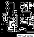
Below are photos of boards made by PCBExpress

 
Last edited:

jpanhalt

Joined Jan 18, 2008
11,087
First, not all photoresists are the same. Some can be developed with sodium carbonate or sodium silicate, some cannot. The brand I use from DigiKey (Injectorall, http://www.digikey.com/product-search/en/prototyping-products/accessories/2359380?k=INjectoral) cannot be developed with anything less basic than NaOH or KOH. Since the basic chemistry is about the same, i.e., a Novolac resin and a photosentizer, the differences are probably in the photosensitizer and concentrations used.

Second, the best printer in my opinion for the photoresist mask is a good ink jet. It doesn't have to be black. All of the colors block the near UV (UVA) required. Since I now make boards so infrequently, I stopped using the inkjet, because the ink cartridges dried out between uses. I use a laser printer, and rather than layer multiple copies to get adequate density to prevent pin-holing, I just paint over the transparency with a dry erase marker. After that dries, I wipe off the excess with soft tissue. The marker fills the voids and is not removed by the wiping with tissue (Kleenex). Unfortunately, I discovered last year that not all toners will work with that method. HP works great and was the printer I used to develop the method. Brother works poorly. The difference can be seen with a magnifying glass. HP is fine particles. Brother is more like paint splotches.

I develop in dilute caustic soda (NaOH or KOH, about 0.4 molar) and etch with ferric chloride or cupric chloride. I found that the peroxide-based etchants (e.g., H2O2 _HCl) attacked the resist that I use.

I used to use the immersion tin coating, but stopped doing that years ago. Here is an example of a board I made last year with that method:

upload_2015-3-2_15-48-36.png

Here's an example of the dry erase transparency treated and untreated:

upload_2015-3-2_15-50-49.png

Here's a closer view from another project after the dry erase treatment:

upload_2015-3-2_15-58-8.png

And here's the completed board from that transparency:

upload_2015-3-2_15-59-45.png

I don't use thin traces, unless necessary. I estimate the name ("zero width") is about 4 mil or so. I like ferric chloride/cupric chloride because of the sharp edges with minimal undercutting that they give. I have a close up somewhere, but couldn't find it right now. If I do, I will add it to this post.

John
 

Thread Starter

Lestraveled

Joined May 19, 2014
1,946
John
Your boards look great! I never thought of using dry erase markers. I will try that.

I agree on using thick traces over thin. No need to make traces thin unless it is really needed.
 

Thread Starter

Lestraveled

Joined May 19, 2014
1,946
John
I tried your dry erase marker thing to darken the laser transparency. It darken the image but it also removed laser toner. I tried different ways to apply it but I could not get it to work.


jpanhalt

Joined Jan 18, 2008
11,087
I suspect you are not using a LaserJet by HP. My Brother is a great printer, but its fusing temp (?) seems to be lower and the toner is not stable to the dry erase. I got the same sort of results you got. The HP toner is really durable. Since toner doesn't dry out, I am trying to find a place for my HP 4100 MFP. It is/was an expensive and large tank, but works well with the dry erase variation. Brother and HP are the only two manufacturers with which I have experience.

Actually, starting last year, I have pretty much gone to commercial board houses, unless I need something simple in a hurry.

John
 

Thread Starter

Lestraveled

Joined May 19, 2014
1,946
John
Yes, I am using an HP 1160. I get my best density with after marker toner cartridges. I put an HP toner cartridge back in and re-tried the dry erase marker. No difference.

I know what you mean about commercial board houses. They have made it so easy, especially PCBExpress. I can still make boards 1/5 to 1/10 the price.
 

jpanhalt

Joined Jan 18, 2008
11,087
Hi Les,

What brand of marker do you use? I will try it with my HP4100 to see if it is the marker or the toner. Deep down, I suspect it is the toner. The newer toners appear to be low temperature versions (energy saving?) of the earlier toners.

As for cost, I just ordered 5 ITEAD boards, 5cmX10cm for $21.33 total, including shipping. I could not make five boards for that price, including shipping. In fact, one board including shipping would come to about half that. Time and quality will tell.

There will always be times when someone wants a DIY board. So, I think putting down a reasonable procedure for using the photoresist method is a worthwhile project. I have never gotten the toner transfer method to work to my standards.

Regards, John
 

Thread Starter

Lestraveled

Joined May 19, 2014
1,946
The dry erase marker I have is a "Messagestor'. It is alcohol based. From the MSDS sheets, most dry erase markers are alcohol based. The "Quartet Duraglide" DE markers appear to be water based. I will try to find some of these.
 

jpanhalt

Joined Jan 18, 2008
11,087
I will try to find the Messagestor brand. The brand I use is Expo from Office Depot. It has a chisel tip rather than pointed. Here's an MSDS for it: https://store.schoolspecialty.com/OA_HTML/xxssi_ibeGetWCCFile.jsp?docName=G616260

Pink has a different MSDS. One thing I should have mentioned is that the black ink seems to behave like a pigment (it becomes a powder when removed); whereas, the others seem to have more dissolved color (i.e., dyes) in them. The colors other than black are more difficult to erase from a white board and do not work in the PCB method either. Expo is sold as "low odor". It is quite possible that the black version has more water in it than the other colors. Water content may not be listed on an MSDS. Anyway, I will try to find the brand you used and test it with my HP printer. That may be a few days, as my next trip into Cleveland won't be until the weekend.

A water-based marker should work better than one that has only alcohol as the carrier.

John
 

Thread Starter

Lestraveled

Joined May 19, 2014
1,946
OK, a small update on the dry erase marker issue.

The dry erase markers that contain alcohol or ethanol, take the toner off of the transparencies.
The brands that the above includes are: Expo, Officemax, MessageStor, and Crayloa.

I also tested blue food coloring. It did remove some of the toner. I suspect that it was the Propylene Glycol in it.

I tested tap water. It did not remove any toner at all.

Through the MSDS, I identified that the "Quartet Enduraglide" dry erase markers are alcohol and ethanol free. There are no stores in Tucson that carry them so I ordered some through Amazon. They will arrive Wednesday.

If a simple procedure like applying a dry resist marker to the transparency will greatly improve the density, then the printer to PCB path will get much shorter and simplier. Lets hope.

Come on, lets heard some more ideas.
 

Thread Starter

Lestraveled

Joined May 19, 2014
1,946
I received the Quartet Enduraglide water based dry erase markers today and below are the results.

Left image: untouched laser image. Right: Image treated with the Quartet Enduraglide markers.


My evaluation
The water based maker worked better that the alcohol/ethenol based markers. With a very gentle hand, I was able to treat the image without removing any toner, which was a problem that the alcohol markers had. Unfortunately, when removing the marker pigment with a soft cloth or a Q tip, the toner would often come off also.

Conclusion - At first, I was excited about the concept of darkening the image with some kind of ink/pigment. Now, I am not so enthusiastic. I can see that dry erase markers would be good for touch up on small simple boards, in that, if you messed up your touch up, you had a good chance of fixing it. But, I think dry erase markers fail as a wholesale darkening agent for large boards.

Now, how am I going to use all of these markers before they dry out.
 

atferrari

Joined Jan 6, 2004
4,767
WOW, WOW, WOW! Impressive; so much knowledge in play.

Sorry gentlemen. You have experimented a lot. But I am still thinking that I would be happy to get a PCB drilling machine for prototypes. I simply did not buy it (Stepcraft 300) because I run short of time to reach Germany and then catch my flight back home.

After watching locally, a demonstration with a LPKF machine (authorized dealer), I had it in my mind all the time.

/EDIT
it is "PCB milling" machine
EDIT/
 
Last edited:
Top