Project: LED based UV exposure box for PCBs

Thread Starter

Markd77

Joined Sep 7, 2009
2,806
Materials:
A CD case, some wood, 20 "UV" LEDs, a few resistors, cardboard, aluminium foil, stripboard.
The "UV" LEDs are not really UV, they are violet and fairly cheap on eBay - I got mine from Phenoptix. The wavelength is 400nm.
The pictures explain it fairly well, I'm using 12V from my bench power supply and the LEDs are connected in parallel chains of 3 and one of 2 with current limiting resistors. I measured and matched the forward voltages of the chains of 3 LEDs to hopefully reduce the brightness variation. As LEDs vary I'm not mentioning resistor values.
I printed on transparency paper with an inkjet and the density of the print isn't great but still ended up with usable results. I may experiment with a double layer of transparency. A book on top of the transparency and PCB holds it flat.
I get the best results with an exposure time of 3 minutes with the PCB I'm using.

If I was doing it again I would attach the LEDs to stripboard, it would save a lot of time.


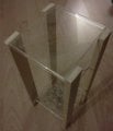
Hot glue is used to attach the CD case to the wood. It's about 30cm high to spread the beams from the LEDs out so they overlap.


I used epoxy putty (milliput) to hold the LEDs in place.


The surround is cardboard with a sheet of aluminium foil attached. It helps level the brightness out.


Fairly even coverage.


The result: not perfect but useable. The main traces are 20/1000 inch or about 0.5mm and the pad outline at the center right is 10/1000 inch or about 0.25mm
 

Attachments

nerdegutta

Joined Dec 15, 2009
2,684
Nice!

A couple of questions:

What is controlling the exposure time?

What is the size of the PCB you can exposure?

What do you use the develop the PCBs?
 

Thread Starter

Markd77

Joined Sep 7, 2009
2,806
The timing is manual, I didn't think it was worth adding a timer and accuracy isn't very important.
Maximum size is 13cm X 11cm.
I'm using a sodium silicate photoresist developer and sodium persulphate etchant.
 

nerdegutta

Joined Dec 15, 2009
2,684
When I made my UV-LED box, I added a PIC to control the time. It gives a buzz, when the time is up. That way I don't have to time it. The exposure time is selected with a turn-switch.

I'm using two transparent printouts. The alignment of the two sheets can be a challenge, but after a few times, I got the hang of it. Instead of a book, I'm using a small piece of glass and I put some weight on top. I have some scrap lead for that.

Thanks for sharing. :)
 

jpanhalt

Joined Jan 18, 2008
11,087
It looks like a bit of over exposure, but I suspect the real culprit may be the etchant. The per<x> etchants eat my photoresist (Injectorall). I am sure your resist chemistry must be a little different, as sodium silicate will not remove the Injectorall resist, but the chemistry is quite similar. Can you get ferric chloride? It may not be your final etchant, but it eliminates a few variables.

As for your inkjet image, have you set ink flow to heaviest? Does the transparency show any beading of the ink?

John
 

Thread Starter

Markd77

Joined Sep 7, 2009
2,806
I think the main problem that is causing the pitting is the low density of the printout. My printer is an old Lexmark that there aren't proper drivers for on Linux (and none at all on Vista). There are visible holes in the black of the print (with a microscope). I think with a better printer the setup would work fine. The PCB is usable so I might not get a new printer just yet - I'm a cheapskate.
 

jpanhalt

Joined Jan 18, 2008
11,087
I messed around with several OHP (over head projector) films before settling on one made by Pictorico. The polyester backing needs to be treated with something to allow the water-based inks to stick. Otherwise, they just bead up microscopically. Pictorico has some sort of microcrystalline coating on it. You get very fine resolution. The ink flows well on it. Main problem is that it is used in commercial arts, and UV hurts the contrast. So, the manufacturer (Mitsubishi) came up with an "improved" version that blocks UV. That's not good for us. I recommend the original, "Pictorico Premium OHP Transparency Film." It is made in Japan. See: pictorico.com. I suspect there are other products out there that will work as well, but this product definitely gives better resolution than the cheap OHP films available in the US.

John
 

nerdegutta

Joined Dec 15, 2009
2,684
What width is the traces? I've tried 0.2mm, but with my current laser printer setup, it won't get dark enough, so I've ended up with 0.4mm. Haven't tried 0.3mm - yet.

Side note:
Once I ran out of transparent film, so I printed the PCB on a regular paper, and soaked it in vegetable oil. It looked like this:


This circuit is drawn in KiCad, and not so good. The finished board is this:

Not my best work, and I've learned a lot since then. :)
 

R!f@@

Joined Apr 2, 2009
9,918
I hate u guys.... U are doing what I cannot. and I want to do this rather badly.

OK..I don't hate you..Love what you have done.
I cannot get wax paper, I cannot get ferric easily..

So what will be the easiest way for me to etch PCB's....I think I can buy ferric balls kinda a thing that should be added to water to make the chemical....I heard this from someone.
Some one really need to give me some heads up on what is the best method for me...
I can buy UV leds off ebay. so Mark..any pointers?
 

Thread Starter

Markd77

Joined Sep 7, 2009
2,806
I edited the post to put in some dimensions.
There are hundreds of LEDs on your setup Nerdegutta, I'm guessing your exposure time is very quick.
Riaff, I think that if you can't get FeCl or wax paper then the alkaline developer, the photosensitive boards and the transparency paper could be hard to get too (and you still need FeCl or some kind of etchant). How's the CNC milling machine you were building going? That could be an option, I've seen boards made that way that look good.
 

jpanhalt

Joined Jan 18, 2008
11,087
Hi Mark,

As you may have gathered, I use the photoresist method and an inkjet for my transparencies. I use only a single layer of transparency and place the ink side of the image against the PCB. I also usually make multiple copies of a pattern to fill of the blank board. I am attaching two pictures of some old boards -- the extras that weren't used. NB: I do not remove the resist until I am ready to solder components to the board. What you are seeing is old resist with a little flaking and accumulated dirt from 2 to 3 years of sitting on my desk. Nevertheless, you should be able to see the sharp etching outline of the copper. Most traces are 24 mil, the out of focus border in one image is 10 mil. I always put a border for a "trim to" line. Your system should be able to do the same. I know of no difference in final results between MG and Injectorall users. I need a better camera for macro shots. :)

John
DSCN1200.jpg

DSCN1200.png
 

nerdegutta

Joined Dec 15, 2009
2,684
...
There are hundreds of LEDs on your setup Nerdegutta, I'm guessing your exposure time is very quick.
...
This picture was from my first setup. A converted flatbed scanner, with a 555 timer. Exposure time, I think was about 7 or 8 minutes. This is now retired.

I've made a new box with a PIC and fewer LEDs. Exposure time now is 10 minutes. It's soon retired too. I'm constructing, in my head for now, a setup which do 2-sided boards. I have all the components, just need to figure out the wood-box...
 

t06afre

Joined May 11, 2009
5,934
Then I had access to pro equipment I could go down to 12 mils tracks. Class 1 PCB was no problem. However could not do much rework on thin tracks before the copper and the pcb plate delaminated. And without a pad as anchor the track was goner. It was just to rip it of, and accept the loss
 

jaclement

Joined Apr 15, 2009
35
Re etchant: 2 parts of hydrogen peroxide plus 1 part of muriatic acid (HCl) make a better etchant. muriatic acid is avalible at hardware stores and H2O2 at pharmacies.
 

Wendy

Joined Mar 24, 2008
23,415
Also a lot more hazardous on a personal level. I use it myself, but it is important to note.

How many people buy pre-coated boards with the photosensitive coating vs. DIY? As I understand it you need to sensitize the board, expose this (this project), then develop it. This is the processes I have problems with. Any good links?
 

jpanhalt

Joined Jan 18, 2008
11,087
In answer to the part about applying a photoresist there are three options:
1) Buy pre-sensitized plates
2) Buy a photosensitive film that the user laminates onto the copper PCB
3) Spreading liquid resist on the copper PCB DIY

I buy pre-sentized boards. They are "positive resist" in the sense that the parts of the transparency that are clear are the parts that are removed during photo-development. In other words, the transparency image is a positive. I believe (without real data) that buying pre-sensitized boards is the most common method.

DuPont has a film material, "Riston" that is laminated onto the bare copper to produce a sensitized board. It was patented in about 1968. I believe the original was a negative resist, but both positive and negative films may be made today -- not sure. MG Chemicals also sells an iron-on negative resist. From what I have read, this is a practical method, just not as popular at the moment as the pre-sensitized boards. For many years, DuPont focused only on the commercial producers. I tried and failed at buying anything less than a 1000-year supply several years ago. I think in the future, DIY'ers wanting specialized boards and thickness may switch to the iron-on photosentizers. I count myself in that group.

Finally, there is the DIY coating. Last time I looked, they were not available from my usual suppliers and for good reason. Doing your own coating this way made about as much sense as making your own Kodak film. Getting a reproducibly thin, even film is just not that simple for DIY'ers. Spraying and brushing were not practical. Dipping and spinning were the most practical (my commercial supplier uses dipping).

John
 

nerdegutta

Joined Dec 15, 2009
2,684
I buy PCB's with positive photoresist.

After exposing them, with UV-LEDs, I develop them with Sodium hydroxide (NaOH), and further to Na2S2O8.
 

Thread Starter

Markd77

Joined Sep 7, 2009
2,806
I use the presensitised boards too.
I need to do more experimenting with different transparencies because the one I got isn't working very well with my printer. I think a double layer would work fine but at £1 a sheet it gets expensive.
The ink seems to shrink and crack on this transparency (the "0" is about 2mm high).
 

Attachments

Top