problem with amplifier assignment

Ylli

Joined Nov 13, 2015
1,092
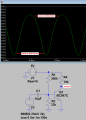
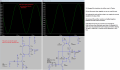
I think you are expecting too much of this simple circuit. The depressed positive going output is due to the fact that you run out of drive when the output increases. Research "Bootstrap". As for the distortion.. probably as good as you could expect from a circuit that is compressing the positive going output and has no feedback.
 

MisterBill2

Joined Jan 23, 2018
27,508
With no input signal the positive side of C3 should be resting at half the supply voltage, which means that also the connection between the emitters of the 2 bias transistors should be close to that half supply voltage point. The driver transistor should be biased to a point half way between cutoff and saturation. Presently I am suspecting that the emitter resistor of the driver transistor is a higher value than it should be, and that it is biased much more toward one end of the curve that the other end.
 

crutschow

Joined Mar 14, 2008
38,503
The problem is that the output has a positive peak of 1.6 volts and a
negative peak of -2.0 volts.
They are near equal at about 1.9V in my simulation using your test parameters.
(I did have to substitute the non-C version the the transistors since I didn't have the C version models).

upload_2019-4-8_19-29-7.png

The THD is a horrible 6.85%.
My simulation measured a little over 3% total.
A push-pull output stage without negative feedback will have a lot of distortion due to transistor non-linearity and crossover distortion.
I have a similar stage using a op amp driver with negative feedback, and the distortion is under 0.2%.
 
Last edited:

ScottWang

Joined Aug 23, 2012
7,501
Please go to google the class-a amplifier, class-b amplifier, mini transistor amplifier, and to see what kind of circuit will affects the stabilize of the circuit.
 

Thread Starter

newbie2019

Joined Apr 5, 2019
95
They are near equal at about 1.9V in my simulation using your test parameters.
(I did have to substitute the non-C version the the transistors since I didn't have the C version models).

View attachment 174567

My simulation measured a little over 3% total.
A push-pull output stage without negative feedback will have a lot of distortion due to transistor non-linearity and crossover distortion.
I have a similar stage using a op amp driver with negative feedback, and the distortion is under 0.2%.

Thanks. crutschow, I will try to find the non-C transistor models. I have heard that some of these models have problems.

I replaced transistors with BD139C and BD140C s and the THD dropped to 0.7%.
 
Last edited:

Thread Starter

newbie2019

Joined Apr 5, 2019
95
Crutschow, the output voltage is +1.63V and -1.55V. I am trying to find some
good info re "negative feedback" and how to implement it.
 

Audioguru

Joined Dec 20, 2007
11,248
NOBODY makes an audio amplifier like that one that has no AC and DC negative feedback (except fuzz producing geetar amplifiers).
Without DC negative feedback then transistor T3 will conduct too much if its hFE is high and it will conduct too little if its hFE is low.
The distortion will be high without AC negative feedback.

Here is a simulated transistor with a high output level (but it is not clipping) and it has no negative feedback, its distortion is extreme:
 

Attachments

MisterBill2

Joined Jan 23, 2018
27,508
NOBODY makes an audio amplifier like that one that has no AC and DC negative feedback (except fuzz producing geetar amplifiers).
Without DC negative feedback then transistor T3 will conduct too much if its hFE is high and it will conduct too little if its hFE is low.
The distortion will be high without AC negative feedback.

Here is a simulated transistor with a high output level (but it is not clipping) and it has no negative feedback, its distortion is extreme:
The negative feedback in a circuit like this one can be as simple as an emitter resistor. Not everybody realizes that they provide local negative feedback, but that is the purpose of emitter resistors. And sometimes we see a more elaborate arrangement of two resistors in series as the emitter resistance, with a capacitor across one of them. That is for when the AC feedback and the DC feedback need to be different. The math is sort of complex in that there are several terms, but the implementation is simple.
 

Audioguru

Joined Dec 20, 2007
11,248
Yes, an emitter resistor provides some AC and DC negative feedback. It is difficult to see 2% to 5% distortion on a 'scope so I showed the extreme distortion of a transistor with no negative feedback. But even though the output transistors are emitter-followers they also produce some distortion.
I think the assignment to find out what is the problem with this amplifier circuit is that it has no all-around AC and DC negative feedback.
Maybe the student is supposed to show it with the negative feedback?
 

Thread Starter

newbie2019

Joined Apr 5, 2019
95
Thanks for the input guys. Big help. I added negative feedback to Q3 and now
the THD is 1.8% and the output voltage is 687mV, Iload = 85.9mA and the pout = 59mW.

It is weird because the output power is 97mW per the transient analysis.
 

Attachments

Last edited:

Audioguru

Joined Dec 20, 2007
11,248
Your circuit still does not have AC and DC negative feedback from its DC output to its DC input.
Negative feedback reduces its distortion and voltage gain.
OOPS! We missed the Monday deadline but I was away all weekend..
I fixed this amplifier:
 

Attachments

Last edited:

MisterBill2

Joined Jan 23, 2018
27,508
I am wondering what the fault that the instructor claimed was present was. Quite a bit has been changed, and a number of flaws corrected, but which one was the planted one to fix? OR could it have been a mixture of many?
 

Thread Starter

newbie2019

Joined Apr 5, 2019
95
I am wondering what the fault that the instructor claimed was present was. Quite a bit has been changed, and a number of flaws corrected, but which one was the planted one to fix? OR could it have been a mixture of many?
The instructor stressed the lack of feedback and the base bias of Q3 as problems. I asked about the use of power transistors
for the bias network and he said they were only used to attempt to match the output transistors. I guess a vbe multiplier would be a better choice. I really learned some things but I know that I have a lot to learn plus I need to gain experience.
 

Thread Starter

newbie2019

Joined Apr 5, 2019
95
NOBODY makes an audio amplifier like that one that has no AC and DC negative feedback (except fuzz producing geetar amplifiers).
Without DC negative feedback then transistor T3 will conduct too much if its hFE is high and it will conduct too little if its hFE is low.
The distortion will be high without AC negative feedback.

Here is a simulated transistor with a high output level (but it is not clipping) and it has no negative feedback, its distortion is extreme:
Thanks Audioguru I will study this one.
 

Audioguru

Joined Dec 20, 2007
11,248
Sorry AG but it seems you won't pass this semester.
The value of R3 was much too high then transistor Q4 could not swing high enough. I reduced its value to 0.22 times the original value.
My last circuit had overall negative feedback, an output of 1W into 8 ohms just before clipping and very low distortion. I pass.
 

crutschow

Joined Mar 14, 2008
38,503
My last circuit had overall negative feedback, an output of 1W into 8 ohms just before clipping and very low distortion. I pass.
Perhaps I'm missing something, but that circuit (post #32) seems to go against your oft stated preference to not have a circuit's operation be sensitive to transistor gain, however its bias point/current appears to depend upon the gain of Q3.
 

Audioguru

Joined Dec 20, 2007
11,248
Perhaps I'm missing something, but that circuit (post #32) seems to go against your oft stated preference to not have a circuit's operation be sensitive to transistor gain, however its bias point/current appears to depend upon the gain of Q3.
Of course this simple amplifier is a little sensitive to the hFE of Q3, but it is fairly small so you will barely notice it.

The datasheet of the 2N3904 shows that its hFE minimum is 1/3rd of its maximum.
1) If the circuit has the junction of the 0.33ohms emitter resistors of the output transistors at half the supply at 6.0V then the hFE is 244.
2) If the hFE is minimum at 122 then the 0.33ohms resistors junction is 7.0V.
3) If the hFE is maximum at 366 then the 0.33ohms resistors junction is 5.0V.

So the maximum undistorted output power with minimum hFE is 0.56W, the power is 1W when the hFE is typical and again the power is 0.56W when the hFE is maximum. 0.56W sounds only a little less loud than 1W.
You can add an emitter resistor to reduce the power differences but the resistor will reduce the maximum output swing and reduce the maximum power.
 

MrAl

Joined Jun 17, 2014
13,702
Hi,

Yes the value of C3 was too small.

Also, the values of R5 and R6 are way too small. 0.001 ohms only drops 0.001 volts at 1 amp peak. That's not enough to help equalize the base emitter drops in case of some mismatch and thus bias current could be high. A better value would be 0.1 ohms.
 
Top