Problem of ondulation in downconverter chain

Thread Starter

BRUNET Joss

Joined Nov 1, 2018
38
Hello everybody,

I am new on this forum, so I introduce myself: I'm 20 year old and I am in electronic/RF engineering school in sandwich course in France.

I come towards you because I have some things that I don't understand.

I currently realize a downconverter (800MHz to 500MHz with 5 MHz of band witch) and when I proceed to an analyse with a network analyzer, I get 4 dB of amplitude variation (in the band witch) and it is not ok for my product specification.

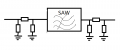
Hardware part details: 800 MHz (+7 dBm) -> Diplexer (Delta amplitude variation: 1.6 dB MAX) -> Mixer (Mini-circuit ADE-2 with Analog Device ADF4360-8 for LO +7 dBm) -> LNA (Mini-circuit PGA-103+) -> SAW filter (500 MHz and Single Ended Operation at 50Ω without matching and amplitude variation: 1.6 dB MAX) -> Amplifier (MMG3006NT1 with network matching realized with auto-match tool in RFsim99) -> SAW filter (500 MHz and Single Ended Operation at 50Ω without matching and amplitude variation: 1.6 dB MAX) -> 500 MHz.

I am looking for advices, like the importance of matching network for PGA-103+ (attachment) or how to calculate the total amplitude variation with two SAW filter similar cascade...

Have a good day!

Joss

Capture.PNG
 
Last edited:

danadak

Joined Mar 10, 2018
4,057
Are you going to connect SAW1 >> Buffer >> SAW2 or just SAW1>> SAW2,
in other words buffer isolation of stages or no isolation ?

If cascading two SAWs follow s parameter analysis to apply -


Regards, Dana.
 
Last edited:

Thread Starter

BRUNET Joss

Joined Nov 1, 2018
38
Hello Dana and thanks for your answer.

I understood that the s parameter is not the same if cascading two SAWs filters. But I don't have the s parameter of the filter and in my actually design, I don't have two SAWs filters cascading. Maybe that the problem is with the MMG3006NT1 cascading?

I drew a block diagram of actually hardware (attachment). All component is matched 50 Ohm except the MMG3006NT1, that's why they are LC circuit.

upload_2018-11-4_16-53-6.png

By experience, tell me if possible, where it is important to add a buffer ?

Regards, Joss.
 

cariban

Joined Aug 14, 2018
69
Hello Dana and thanks for your answer.

I understood that the s parameter is not the same if cascading two SAWs filters. But I don't have the s parameter of the filter and in my actually design, I don't have two SAWs filters cascading. Maybe that the problem is with the MMG3006NT1 cascading?

I drew a block diagram of actually hardware (attachment). All component is matched 50 Ohm except the MMG3006NT1, that's why they are LC circuit.

View attachment 163107


By experience, tell me if possible, where it is important to add a buffer ?

Regards, Joss.
From your diagram I can see that there are several traps. Most difficult part should be related to SAW filter. SAW filter is a narrow band passband filter and thus needs very good impedance matching for both source and load impedance. I would suggest:
1. Add PI-impedance matching network for all input/output for SAW filter and SAW duplexer. Your bandwidth is only 5MHz, the impedance matching should be rather easy;

2. Move one LNA MMG3006NT1 to be between the SAW filter and SAW duplexer in the ouput stage. This provide a buffer between two SAW components;

3. Just have a quick check the datasheet of MMG3006NT1, the noise figure of this chip is quite high. Why do you choose this chip? There are many simpler LNA from Mini-circuits or Qorvo. As I know NXP is not a master for RF components;

4. Measure the performance from start to end in the chain and find out which section causes the problem. Also try to optimize the performance stage by stage;

5. Layout is quite critical at this frequency. Try to find an experienced RF guy to check the layout.
 
Last edited:

Thread Starter

BRUNET Joss

Joined Nov 1, 2018
38
Thanks for your answer Cariban.

1. I have chosen a SAW filter which works without matching network (cf datasheet : Single Ended Operation at 50Ω without matching). So I don't understand how I can add a matching network. Maybe a buffer instead of matching network?

2. OK but I obtain always amplitude variation if I realize the measure without the 500MHz duplexer.

3. Thanks for this advice, I will see to replace the MMG3006NT1. I had chosen the MMG3006NT1 for his high Pout level : +33dBm.

4. Yes, to solve a problem, I use a high impedance probe and I realize the tracking after each component. Perhaps it is better to unplug each component and put a 50 Ohm resistance before realise the tracking?

5. I will try to found an experienced RF guy but for your information, I respected basic rules of routing like impedance line. Also, I have used a "coplanar waveguide with ground" technology and with a very small isolation, the ground (in green) comes under each component:

upload_2018-11-6_18-39-21.png

Each components create an impedance break, the ground return it is a problem ?

Regards, Joss.
 

cariban

Joined Aug 14, 2018
69
1. I have chosen a SAW filter which works without matching network (cf datasheet : Single Ended Operation at 50Ω without matching). So I don't understand how I can add a matching network. Maybe a buffer instead of matching network?
SAW filter needs both source/load impedance to be 50 Ohm. Refer to the attached picture. Note each component of PI impedance matching network could be either inductor or capacitor depending on the matching situation To do in-board impedance match, you need a vector network analyzer. First you measure the actual impedance at the band, then use the PI impedance matching network to obtain 50 Ohm source/load impedance. Your signal is narrow band, so three components are sufficient.

2. OK but I obtain always amplitude variation if I realize the measure without the 500MHz duplexer.
Put amplifier in the middle helps to isolate the SAW components, thus simplify the impedance matching.


3. Thanks for this advice, I will see to replace the MMG3006NT1. I had chosen the MMG3006NT1 for his high Pout level : +33dBm.
It is pretty OK to use MMG3006NT1. I just suggest you to search if there are better choices. "Better" means small footprint, lower noise figure, less power, better returnloss....


4. Yes, to solve a problem, I use a high impedance probe and I realize the tracking after each component. Perhaps it is better to unplug each component and put a 50 Ohm resistance before realise the tracking?
I am not sure you use spectrum analyzer or oscilloscope to measure the RF signal, but I guess you use spectrum analyzer. It is not a good idea to use high impedance probe to check RF signal seriously. You should disconnect the latter chains, then solder a 50 Ohm coaxial cable on the PCB board and connect the cable to the spectrum analyzer. The cable should have good quality and flexible. Also make the cable as short as possible. This is to guarantee the load impedance is close to 50 Ohm since spectrum analyzer has very good returnloss.


5. I will try to found an experienced RF guy but for your information, I respected basic rules of routing like impedance line. Also, I have used a "coplanar waveguide with ground" technology and with a very small isolation, the ground (in green) comes under each component:
Coplanar waveguide is OK. But it may be better to use microstrip for this frequency. Use a proper PCB stack-up to obtain 50 Ohm microstrip track with width about 0.5mm. This size matches well with EIA-0402 component width. After finish the tracks, flooding the component layer with GND plane. Keep the clearance between RF tracks and GND filling 3~5 times of the height to the reference plane. For example if the height of dielectric material is 0.2mm, use 0.6~1mm as clearance to the GND filling.
 

Attachments

Thread Starter

BRUNET Joss

Joined Nov 1, 2018
38
Hello Cariban,

1. Ok, I have understand. Even thought the filter is matched under 50 Ohms, I measure and I adapt the SAW silter with SimSmith (for example).

2. Ok, I have understand too.

3. Yes, of course. I will take more time for my research of component the next time.

4. Ok, I have understand your functionnement. I will create me some RF probes in hard coaxial cable to make more serious measures.

5. After the advice of an experienced guy, my problem is not linked with the CAO. But I take note of your advices.

To resume, after serious measures, my amplitude variation problem is only linked at SAW duplexers. Then it follows that if I need of less amplitude variation, I need to choose an other RF architecture or better SAW filter.

I am very glad to be come onto this forum. This forum and his members are great.
Regards, Joss.
 
Top