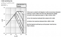
The DC safe operating area of that FET allows about 55 volts drain to source with a current of 1 ampere. That is a power dissipation of 55 watts, which means it will require a large heatsink to cool it sufficiently and limit your maximum VDD to about 65 V depending on exactly how it performs as a source follower. With a supply voltage any higher than that, the FET is unsuitable for continuous current of 1 ampere. See Figure 3 of the datasheet.
1 A with 140 VDD, it it were permissible, would result in around 130 W of dissipation in the FET which would require a very large heatsink or a lot of air flow over a smaller one and make the thermal interface between the package and the heatskink extremely critical.
Thanks for the comments. You are right and in fact I started to look for other Power FET transistor to better fit my needs for Id/Vds.
About power dissipation you are right but problem cannot be avoided and must be considered and managed since this is the requested application
This complete DCDC converter with external fets looks to me really great!
I tried to download models to run your simulation but some are missing and/or not running into LTS environment.
It will be possible for you to send me all models you used in the testbench?
Thank you ivery much!
Although it is certainly possible to produce a buck converter for the requirement, you always have the risk that a short circuit failure in the the FET will apply the full input voltage to the output. For 12 W output, a flyback converter would be much more suitable in my opinion. The circuit is quite simple and removes the issue with a shorted pass device. Power Integrations makes integrated switcher ICs (control and switch in one IC) that are suitable and I think both ON and ST have similar products.
Hi Andrea,
There are a couple of additions I suggest you consider.
Fit a 5Amp fuse in the Drain circuit wiring.
Add a 10K resistor is series with the Gate voltage and connect the Gate to 0V via TVS capable of carrying 5Amps.
If the MOSFET fails without this protection it could take out the Gate driving circuitry.
Finally a reminder, a voltage over 50V can give a shock that can kill.
E
Even though the datasheet for the sum85n15 would make it seem that the part would be suitable, in practical terms it isn't. I regard that datasheet as being very misleading. Try finding some parts with similar ratings in the same package from other manufacturers (or even other Vishay parts) and compare the datasheets.
It is in a very small surface mount package which makes it very difficult to get the heat out of it and into a heatsink. Then there is the problem of removing heat from the heatsink (really a heat dissipator, the ultimate heatsink is air).
[EDIT]: error - the following was calculated using 140 V as the maximum input, not 160 V as actually required
The maximum allowable operating temperature for the actual FET die is 175 °C. At your highest input voltage with 12 volts out, you will be dissipating 128 watts. The thermal resistance from the die to the mounting surface of the package is 0.4 °C/W. That means the die temperature will be 51.2 °C above the mounting surface temperature. The mounting surface would have to be at no more than 124 °C with 128 W. If the ambient temperature is 25 °C, that means you need a thermal resistance in the heatsink of about 99 °C/128 W = 0.77 °C per watt - and that is assuming perfect thermal transfer from the base of the FET to the heatsink. If you can used forced air, 0.77 °C isn't too difficult to accomplish. If you can't use forced air, it will take a large heatsink. The only way you would get anything close to "perfect" heat transfer from the case to the heatsink is if the circuit board were fabricated with a solid copper "slug" that the FET could be soldered to and the slug had holes to allow bolting it to a heatsink. This is possible, but it makes the circuit boards expensive and not many circuit board manufacturers are capable of doing it at all. It also makes soldering of the board difficult because of the large mass of copper that will take much longer to heat and cool than the rest of the board.
Here's the sort of heatsink you would require without using a fan http://www.wakefield-vette.com/Portals/0/resources/datasheets/465,476.pdf
And again, that is if you meet the impossible requirement of perfect heat transfer from the FET package to the heatsink and can allow the FET to operate at its absolute maximum temperature with an ambient of only 25 °C.
I would suggest a FET in a package no smaller than a TO-247. It can be mounted reasonably effectively to a heatsink and if you are very careful 128 watts is not impossible.
This complete DCDC converter with external fets looks to me really great!
I tried to download models to run your simulation but some are missing and/or not running into LTS environment.
It will be possible for you to send me all models you used in the testbench?
Thank you ivery much!
 Facebook
 Google
 GitHub
 Linkedin