I understood now, It's my fault I didn't read the original document very well. it's all given in documents.
I have attached document page 4.
I want to enable Pull Up resistor
Code:
PADCFG1.RDPU = 1;
Can you point out why I am getting error ? member reference base type 'volatile unsigned char' is not a structure or union.
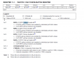
Datasheet PIC18F45K80 Xc8 MPLABX
Hi D,
I guess you know that C1…C4 are set as a High Output and only one C line is switched Low at a time. The C line is switched to Low to ENABLE that Column. So the all the C1 lines are switched Low in turn [ only one C line is Low at any one time]
The 4 Row lines are Input READ lines. [ which are pulled High by either an external resistor or the Internal pull ups on PORTD]
I have written test program to check SW12 but its not working as it should be, When I press SW12, LED doesn't turning ON. I see problem, C1 doesn't change from 1 to 0 when I press SW12
C:
#define _XTAL_FREQ 8000000

#include <xc.h>
// PIC18F45K80 Configuration Bit Settings
// 'C' source line config statements
// CONFIG1L
#pragma config RETEN = OFF      // VREG Sleep Enable bit (Ultra low-power regulator is Disabled (Controlled by REGSLP bit))
#pragma config INTOSCSEL = HIGH // LF-INTOSC Low-power Enable bit (LF-INTOSC in High-power mode during Sleep)
#pragma config SOSCSEL = HIGH   // SOSC Power Selection and mode Configuration bits (High Power SOSC circuit selected)
#pragma config XINST = OFF       // Extended Instruction Set (Enabled)
// CONFIG1H
#pragma config FOSC = INTIO2    // Oscillator (Internal RC oscillator)
#pragma config PLLCFG = OFF     // PLL x4 Enable bit (Disabled)
#pragma config FCMEN = OFF      // Fail-Safe Clock Monitor (Disabled)
#pragma config IESO = OFF       // Internal External Oscillator Switch Over Mode (Disabled)
// CONFIG2L
#pragma config PWRTEN = OFF     // Power Up Timer (Disabled)
#pragma config BOREN = SBORDIS  // Brown Out Detect (Enabled in hardware, SBOREN disabled)
#pragma config BORV = 3         // Brown-out Reset Voltage bits (1.8V)
#pragma config BORPWR = ZPBORMV // BORMV Power level (ZPBORMV instead of BORMV is selected)
// CONFIG2H
#pragma config WDTEN = OFF      // Watchdog Timer (WDT disabled in hardware; SWDTEN bit disabled)
#pragma config WDTPS = 1048576  // Watchdog Postscaler (1:1048576)
// CONFIG3H
#pragma config CANMX = PORTB    // ECAN Mux bit (ECAN TX and RX pins are located on RB2 and RB3, respectively)
#pragma config MSSPMSK = MSK7   // MSSP address masking (7 Bit address masking mode)
#pragma config MCLRE = ON       // Master Clear Enable (MCLR Enabled, RE3 Disabled)
// CONFIG4L
#pragma config STVREN = ON      // Stack Overflow Reset (Enabled)
#pragma config BBSIZ = BB2K     // Boot Block Size (2K word Boot Block size)
// CONFIG5L
#pragma config CP0 = OFF        // Code Protect 00800-01FFF (Disabled)
#pragma config CP1 = OFF        // Code Protect 02000-03FFF (Disabled)
#pragma config CP2 = OFF        // Code Protect 04000-05FFF (Disabled)
#pragma config CP3 = OFF        // Code Protect 06000-07FFF (Disabled)
// CONFIG5H
#pragma config CPB = OFF        // Code Protect Boot (Disabled)
#pragma config CPD = OFF        // Data EE Read Protect (Disabled)
// CONFIG6L
#pragma config WRT0 = OFF       // Table Write Protect 00800-01FFF (Disabled)
#pragma config WRT1 = OFF       // Table Write Protect 02000-03FFF (Disabled)
#pragma config WRT2 = OFF       // Table Write Protect 04000-05FFF (Disabled)
#pragma config WRT3 = OFF       // Table Write Protect 06000-07FFF (Disabled)
// CONFIG6H
#pragma config WRTC = OFF       // Config. Write Protect (Disabled)
#pragma config WRTB = OFF       // Table Write Protect Boot (Disabled)
#pragma config WRTD = OFF       // Data EE Write Protect (Disabled)
// CONFIG7L
#pragma config EBTR0 = OFF      // Table Read Protect 00800-01FFF (Disabled)
#pragma config EBTR1 = OFF      // Table Read Protect 02000-03FFF (Disabled)
#pragma config EBTR2 = OFF      // Table Read Protect 04000-05FFF (Disabled)
#pragma config EBTR3 = OFF      // Table Read Protect 06000-07FFF (Disabled)
// CONFIG7H
#pragma config EBTRB = OFF      // Table Read Protect Boot (Disabled)

__bit Interrupt_Flag_1ms;

#define C1          PORTDbits.RD0
#define C2          PORTDbits.RD1
#define C3          PORTDbits.RD2
#define C4          PORTDbits.RD3

#define R1          LATDbits.LATD4
#define R2          LATDbits.LATD5
#define R3          LATDbits.LATD6
#define R4          LATDbits.LATD7

#define LED         LATBbits.LATB1

void Port_Initialized (void)
{
    // LATx registers
    LATA =  0x00;
    LATB =  0x00;
    LATC =  0x00;
//   LATD =  0x00;
    LATE =  0x00;

//  TRISx registers
    TRISA = 0x00;      // All are output, Unused
    TRISB = 0x00;      // Button connected to RB0
    TRISC = 0x00;      // all are output, Unused
    TRISD = 0x0F;      // LED connected to RD2 pin
    TRISE = 0x00;      // All are output, Unused

    ANCON0 = 0x00;     // set to digital port
    ANCON1 = 0x00;     // Set to digital port
    CM1CON = 0x00;     // Comparator off
    CM2CON = 0x00;     // Comparator off
    ADCON0 = 0x00;     // A/D conversion Disabled
    ADCON1 = 0x00;     // A/D conversion Disabled
    ADCON2 = 0x00;     // A/D conversion Disabled
}

void main(void)
{
    Port_Initialized ();
    PADCFG1 = 0x80;

    R1 = 1; //
    R2 = 1; //
    R3 = 1; //
    R4 = 1; //

    R1 = 0;

    LED = 0;
    while (1)
    {
        if ( C1 == 0)
        {
            LED = 1;
        }

    }
}
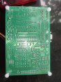
The row and column R1, C1 etc. labels on the PCB are indeed interchanged. Also confusing is that the schematic labels the buttons from 0-15 and the board labels the buttons from 1-16. I traced out the circuit from board photos and here's what it actually is. The PDFs show the actual traced out circuit and resulting schematic.
If you want to interchange the row and column names that would make more sense but update the schematic to show the new labels as well as how the port pins are connected.
Hope that helps.
EDIT 9/15/2021 1337 CDT: The originhal PDF schematic, Keypad As Wired, had the button numbers wrong. Replaced by Keypad As Wired Rev 1 Corrected to agree with the Keypad Rear Wiring scan. Sorry!
@Djsarakar@ericgibbs
The Keypad As Wired schematic in #508 had the button numbers incorrectly listed. The schematic has been revised and re-posted in #508 as well as here.
Here is the corrected info from #508:
R1-C1 should be switch #1as labeled on the board itself (not the original schematic). Use the corrected PDF I posted in #511. For now, use the R and C labels as marked on the board even though they do not correspond to normal rows and columns.
You need to clear PADCFG1<7> to turn on the pullups. You are setting it and turning the pullups OFF.
Each of the PORTD pins has a weak internal pull-up. A
single control bit can turn off all the pull-ups. This is
performed by setting bit, RDPU (PADCFG1<7>). The
weak pull-up is automatically turned off when the port
pin is configured as an output. The pull-ups are
disabled on all device Resets.
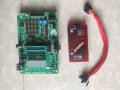
I would test the keypad matrix using the PK3 debugger and some test code.
Write a test sequence that does this:
Init
Set a breakpoint right after init. All of the 'R' lines are 1. Measure the voltage on each of the 'C' inputs. Each should be 5V if the pullups are working. Press a few buttons, there should be no change in the voltage on the 'C' pins because there are no 'R's set to 0 to pull them down.
Set RD4 to 0 (R1=0) and break after that to hold R1=0 while you measure. Press buttons 13,9,5,1 in sequence and verify that a 0 appears on the corresponding, correct port input (RD3-RD0) for each one. Press some other buttons that are driven by the other 'R' lines.
Continue by selecting the other 'R' outputs, breaking after each one and ensure that the corresponding 'C' buttons show up on the proper pins. Refer to the PDF actual wiring schematic I posted.
Once you have confirmed that all of the buttons show up at the correct R-C intersection, you can code the rest.
Example:
C:
LATD = 0xFF;   // Init: set all 'R' = 1.
asm("nop");   // break here and test  button 'C' lines.
LATD = 0b11101111; // R1 (RD4) = 0;
asm("nop");   // break here and test the button 'C' lines on RD3-RD0 = 13,9,5,1 respectively.   1 = open, 0 = pressed.  No other buttons should show up on the 'C' lines.
LATD = 0b11011111; // R2 (RD5) = 0;
asm("nop");   // break here and test the button 'C' lines on RD3-RD0 = 14,10,6,2 respectively. .  1 = open, 0 = pressed.
LATD = 0b10111111; // R3 (RD6) = 0;
asm("nop");   // break here and test the button 'C' lines on RD3-RD0 = 15,11,7,3 respectively. .  1 = open, 0 = pressed.
LATD = 0b01111111; // R4 (RD7) = 0;
asm("nop");   // break here and test the button 'C' lines on RD3-RD0 = 16,12,8,4 respectively. .  1 = open, 0 = pressed.
Once you can see each button individually as the 'R' lines are scanned, you can proceed to coding the scanning etc. If you don't get the expected results, recheck the wiring until you do. Again, all references are to the actual board markings.
I added PORTD pins to the corrected schematic.
Also, the answer to this from #510 is now #1, not #13.
R1-C1 should be switch #1 13as labeled on the board itself (not the original schematic). Use the PDF I posted in #508. For now, use the R and C labels as marked on the board even though they do not correspond to normal rows and columns.
Set a breakpoint right after init. All of the 'R' lines are 1. Measure the voltage on each of the 'C' inputs. Each should be 5V if the pullups are working. Press a few buttons, there should be no change in the voltage on the 'C' pins because there are no 'R's set to 0 to pull them down
There appears to be a typo in the Microchip information I posted earlier. RDPU needs to be ‘1’ to enable pull-ups on the inputs. So your original PADCFG1=0x80 is probably correct.
See Register 11-1 in the datasheet.
The ‘R’s need to start at 1 and the RDPU description says that pull-ups are also controlled by the latch value. That may refer to the TRIS or it actually wants specific value written to the LATx input pin to control the pull-up. I am not real sure and can’t test it right now.
CN9?
The 4x4 matrix has nothing to do with CN9. That connector is for the individual buttons.
The keypad requires only the 4 output lines and the 4 pulled up input lines from the PIC. No power connection.
@JohnInTX@hexreader
I have tested keypad key 1. I have uploaded test code and its working for me. Now Next I am going to make useful project with LCD and Keypad using timer interrupt. I'm busy today, so tomorrow I'll write code
C:
#define _XTAL_FREQ 8000000

#include <xc.h>
// PIC18F45K80 Configuration Bit Settings
// 'C' source line config statements
// CONFIG1L
#pragma config RETEN = OFF      // VREG Sleep Enable bit (Ultra low-power regulator is Disabled (Controlled by REGSLP bit))
#pragma config INTOSCSEL = HIGH // LF-INTOSC Low-power Enable bit (LF-INTOSC in High-power mode during Sleep)
#pragma config SOSCSEL = HIGH   // SOSC Power Selection and mode Configuration bits (High Power SOSC circuit selected)
#pragma config XINST = OFF       // Extended Instruction Set (Enabled)
// CONFIG1H
#pragma config FOSC = INTIO2    // Oscillator (Internal RC oscillator)
#pragma config PLLCFG = OFF     // PLL x4 Enable bit (Disabled)
#pragma config FCMEN = OFF      // Fail-Safe Clock Monitor (Disabled)
#pragma config IESO = OFF       // Internal External Oscillator Switch Over Mode (Disabled)
// CONFIG2L
#pragma config PWRTEN = OFF     // Power Up Timer (Disabled)
#pragma config BOREN = SBORDIS  // Brown Out Detect (Enabled in hardware, SBOREN disabled)
#pragma config BORV = 3         // Brown-out Reset Voltage bits (1.8V)
#pragma config BORPWR = ZPBORMV // BORMV Power level (ZPBORMV instead of BORMV is selected)
// CONFIG2H
#pragma config WDTEN = OFF      // Watchdog Timer (WDT disabled in hardware; SWDTEN bit disabled)
#pragma config WDTPS = 1048576  // Watchdog Postscaler (1:1048576)
// CONFIG3H
#pragma config CANMX = PORTB    // ECAN Mux bit (ECAN TX and RX pins are located on RB2 and RB3, respectively)
#pragma config MSSPMSK = MSK7   // MSSP address masking (7 Bit address masking mode)
#pragma config MCLRE = ON       // Master Clear Enable (MCLR Enabled, RE3 Disabled)
// CONFIG4L
#pragma config STVREN = ON      // Stack Overflow Reset (Enabled)
#pragma config BBSIZ = BB2K     // Boot Block Size (2K word Boot Block size)
// CONFIG5L
#pragma config CP0 = OFF        // Code Protect 00800-01FFF (Disabled)
#pragma config CP1 = OFF        // Code Protect 02000-03FFF (Disabled)
#pragma config CP2 = OFF        // Code Protect 04000-05FFF (Disabled)
#pragma config CP3 = OFF        // Code Protect 06000-07FFF (Disabled)
// CONFIG5H
#pragma config CPB = OFF        // Code Protect Boot (Disabled)
#pragma config CPD = OFF        // Data EE Read Protect (Disabled)
// CONFIG6L
#pragma config WRT0 = OFF       // Table Write Protect 00800-01FFF (Disabled)
#pragma config WRT1 = OFF       // Table Write Protect 02000-03FFF (Disabled)
#pragma config WRT2 = OFF       // Table Write Protect 04000-05FFF (Disabled)
#pragma config WRT3 = OFF       // Table Write Protect 06000-07FFF (Disabled)
// CONFIG6H
#pragma config WRTC = OFF       // Config. Write Protect (Disabled)
#pragma config WRTB = OFF       // Table Write Protect Boot (Disabled)
#pragma config WRTD = OFF       // Data EE Write Protect (Disabled)
// CONFIG7L
#pragma config EBTR0 = OFF      // Table Read Protect 00800-01FFF (Disabled)
#pragma config EBTR1 = OFF      // Table Read Protect 02000-03FFF (Disabled)
#pragma config EBTR2 = OFF      // Table Read Protect 04000-05FFF (Disabled)
#pragma config EBTR3 = OFF      // Table Read Protect 06000-07FFF (Disabled)
// CONFIG7H
#pragma config EBTRB = OFF      // Table Read Protect Boot (Disabled)

__bit Interrupt_Flag_1ms;

#define C1          PORTDbits.RD0
#define C2          PORTDbits.RD1
#define C3          PORTDbits.RD2
#define C4          PORTDbits.RD3

#define R1          LATDbits.LATD4
#define R2          LATDbits.LATD5
#define R3          LATDbits.LATD6
#define R4          LATDbits.LATD7

#define LED         LATBbits.LATB1

void Port_Initialized (void)
{
    // LATx registers
    LATA =  0x00;
    LATB =  0x00;
    LATC =  0x00;
    LATD =  0xFF;
    LATE =  0x00;

//  TRISx registers
    TRISA = 0x00;      // All are output, Unused
    TRISB = 0x00;      // Button connected to RB0
    TRISC = 0x00;      // all are output, Unused
    TRISD = 0x0F;      // LED connected to RD2 pin
    TRISE = 0x00;      // All are output, Unused

    ANCON0 = 0x00;     // set to digital port
    ANCON1 = 0x00;     // Set to digital port
    CM1CON = 0x00;     // Comparator off
    CM2CON = 0x00;     // Comparator off
    ADCON0 = 0x00;     // A/D conversion Disabled
    ADCON1 = 0x00;     // A/D conversion Disabled
    ADCON2 = 0x00;     // A/D conversion Disabled
}

void main(void)
{
    Port_Initialized ();
    PADCFG1 = 0x80;

    R1 = 1; //
    R2 = 1; //
    R3 = 1; //
    R4 = 1; //
    asm("nop");
    R1 = 0;

    LED = 0;
    while (1)
    {
        if ( C1 == 0)
        {
           LED = 1;
           __delay_ms(1000);
            LED = 0;
           __delay_ms(1000);


        }
    }
}
 Facebook
 Google
 GitHub
 Linkedin