PCB Help Needed

Thread Starter

Evan_g

Joined Apr 29, 2024
11
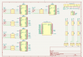
I hope you are doing well. I'm a high school student and am in the process of designing a simple PCB through KiCad for a project I'm working on. This is my first time dipping my toes in any sort of electrical engineering so although the countless tutorials I watched helped me get started I'm a little lost when it comes to creating a working circuit. I'm looking for anyone who has some experience in this field to help guide me through the process of creating my first board and help it all make sense. I dropped a screenshot of the schematics for the board in progress down below.

FYI: I'll give more specifics on the project to anyone interested in helping!
 

Attachments

dl324

Joined Mar 30, 2015
17,227
Your screen capture doesn't enough resolution to be readable.

Some tough love. The style you've used to draw your "schematic" is useless. It's referred to as "connect by name". I refer to it as "netlist" because it's about as easy to read as a schematic netlist.

A thoughtfully drawn schematic will be more useful.

KiCad must have the ability to print to a black and white PDF. That would be much preferable to some "pretty" colored schematic. The professionals never depended on colorful schematics to convey intent.

The schematic editor I use (Eagle) also uses colors. I will rarely post a screen shot of a schematic because the colors are just silly.
 

Thread Starter

Evan_g

Joined Apr 29, 2024
11
Your screen capture doesn't enough resolution to be readable.

Some tough love. The style you've used to draw your "schematic" is useless. It's referred to as "connect by name". I refer to it as "netlist" because it's about as easy to read as a schematic netlist.

A thoughtfully drawn schematic will be more useful.

KiCad must have the ability to print to a black and white PDF. That would be much preferable to some "pretty" colored schematic. The professionals never depended on colorful schematics to convey intent.

The schematic editor I use (Eagle) also uses colors. I will rarely post a screen shot of a schematic because the colors are just silly.
Yeah I agree, another user recommended the "connect by name" method but I soon released it just made the schematic even more confusing so I was planning on changing it back anyways.

In terms of the screenshot I apologize for the sloppiness but honestly, it was quick for me to do and the general aim was to show the progress schematic-wise that I had made. At the time of making this, it was quite late at night so my goal was to come back in the morning and give more in-depth and neater information to anyone interested.

Thank you for your advice nonetheless!
 

dl324

Joined Mar 30, 2015
17,227
another user recommended the "connect by name" method
Connect by name is rarely conducive for conveying circuit intent.

Think about how difficult this schematic would be to read if it used "connect by name":
1719876088354.png
This was a partial redraw of this schematic which was more difficult to read:
Board41schbw1b.jpg
 

dl324

Joined Mar 30, 2015
17,227
On the other extreme, here is an example of a very bad schematic drawing.
I hate that broken line style. They're using connection dots, so they could have just crossed the wires. Even "humps" would have been better. The unnecessary wire jogs screams "amateur" to me. The symbol for the flip flop is terrible.
1719878097630.png
 
Drawing a circuit representing a micro-controller with peripheral circuits is different then drawing discrete digital circuits.
The author has to find a good balance between net name usage and discrete wire connects.
I don't think the TS posted schematic is all that bad, except for readability/resolution.
 
Top