PCB Feedback - 12V Regulator

Thread Starter

alexring

Joined Dec 11, 2022
2
Hi all!

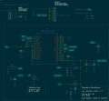
I hope this is the correct place to post this but I was hoping for some feedback on a regulator design I have made.
It's based on the LT8612 (Datasheet: https://www.analog.com/media/en/technical-documentation/data-sheets/lt8612.pdf)

Images of the schematic and layout are attached!

I am very out of practice with PCB design and would love any feedback or criticism you might be able to share!

Thanks kindly in advance,
Alex
 

Attachments

ronsimpson

Joined Oct 7, 2019
3,045
C2 & C7 bump into each other.
The copper "SW" below C2 is thin. Either remove thermals on C2 or turn C2 90 degrees. Increase size of "SW" copper.
Trace to Vout too thin. Make thick or move to near connector. Now I see that is just for testing so it does not matter.
Why remove copper under L1? Copper caries heat away for L1.
There are many places where the grounds have "thermals" to keep heat from flowing. I do not do that. I want to get the heat out of the IC.
C7 is not well connected to ground. I do not what to do about it.
C1 4.7uF 50V can you really find a cap that big in that small package? While you are looking please check C4,5.
I have no thernals on any boards.
1670806712551.png
 

Thread Starter

alexring

Joined Dec 11, 2022
2
C2 & C7 bump into each other.
The copper "SW" below C2 is thin. Either remove thermals on C2 or turn C2 90 degrees. Increase size of "SW" copper.
Trace to Vout too thin. Make thick or move to near connector. Now I see that is just for testing so it does not matter.
Why remove copper under L1? Copper caries heat away for L1.
There are many places where the grounds have "thermals" to keep heat from flowing. I do not do that. I want to get the heat out of the IC.
C7 is not well connected to ground. I do not what to do about it.
C1 4.7uF 50V can you really find a cap that big in that small package? While you are looking please check C4,5.
I have no thernals on any boards.
View attachment 282836
Ron, thanks so much for all your feedback! I really appreciate your time and effort.

I will look through all that you have suggested, especially double checking availability of the components in the packages I have selected!

With respect to thermals, I presume you are referring to thermal reliefs on the pads? I was under the impression that they are desirable on large pours for soldering but I guess this is less of a concern when an oven is used (which I will be)

Thank you again!
 

ronsimpson

Joined Oct 7, 2019
3,045
With respect to thermals, I presume you are referring to thermal reliefs on the pads? I was under the impression that they are desirable on large pours for soldering but I guess this is less of a concern when an oven is used (which I will be)
It is true that hand soldering is harder with no thermals. My boards are soldered in an oven and the entire board is heated to the milting point. Hot air is much the same where you heat a large area at a time.

I circled two VIAs that appear to go no where. You should get an error via to close to hounting hole.
You have PGND and GND connected together on the blue side. You can also connect them on the red side.
These ICs really don't have a place for a heatsink. I try hard to connect as much copper to the IC as a heatsink. I think you could get a better thermal connection if the top side GND and PGND were connected at the IC.
1670815146519.png
Parts are hard to find! Get all the parts on order before you send off for boards. I have to change to different parts almost every day.
 
Top