P-ch MOSFET controlled by μC to drive a load

Thread Starter

Jimis

Joined Jun 15, 2024
15
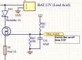
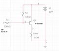
I have the following circuit components on a PCB with an N-channel MOSFET.
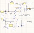
I want to convert the circuit to P-channel MOSFET controlled by an ESP pin with minimum external components. Maybe a few resistors or diodes, I want to avoid another FET.
A problem is that ESP pin won't handle voltages >3.6V even though I could use open-drain (high impedance when not used) I can't be certain that this might not change from SW and damage the pin

Any ideas ?
 

Attachments

ericgibbs

Joined Jan 29, 2010
21,391
Hi Jimis,
Welcome to AAC.
The problem with your circuit is that the PMOS will not switch OFF.
To turn it Off the Gate would have to be +13V.
Have you a general purpose transistors in your parts box.?
E
 

Thread Starter

Jimis

Joined Jun 15, 2024
15
Thanks for the reply Eric.
I understand that a transistor would solve my problem but because the pcb already exists I was thinking if there is a simpler way to avoid difficult components to place like the transistor. Maybe resistors or diodes. The actual circuit on the PCB is the following (N-channel which I want to make P-channel)
 

Attachments

Ian0

Joined Aug 7, 2020
13,097
Thanks for the reply Eric.
I understand that a transistor would solve my problem but because the pcb already exists I was thinking if there is a simpler way to avoid difficult components to place like the transistor. Maybe resistors or diodes. The actual circuit on the PCB is the following (N-channel which I want to make P-channel)
If the pcb already exists then your source and drain pins will be in the wrong place.
 

ElectricSpidey

Joined Dec 2, 2017
3,312
So let me guess...

The original design uses a NMOS as a high side switch and you are not getting the needed voltage at the load.

You need to show more of the schematic.
 

ericgibbs

Joined Jan 29, 2010
21,391
Hi Jim,
As this a prebuilt PCB, I guess you are aware if you do not invert the ESP input signal to the NMOS the output sense into the load will be inverted?
E
 

Thread Starter

Jimis

Joined Jun 15, 2024
15
I didn't want to complicate it but here it is.
Mains power supply feeds U1 and U3 which charges the Lead Acid Bat (1st pic). There is leakage current from the 12V to the battery that's why diode Vdrop is -ve but it's not a problem.

When mains PS is off the circuit (pic 2) still works powering the peripherals from the Lead Acid Bat (although Vgs is -ve !) but the voltage drop at FET is 1.88V. Obviously I had to use a P-ch FET.
 

Attachments

Ian0

Joined Aug 7, 2020
13,097
I didn't want to complicate it but here it is.
Mains power supply feeds U1 and U3 which charges the Lead Acid Bat (1st pic). There is also a charging current from the 12V to the battery that's why diode Vdrop is -ve but it's not a problem.

When mains PS is off the circuit (pic 2) still works powering the peripherals from the Lead Acid Bat (although Vgs is -ve !) but the voltage drop at FET is 1.88V. Obviously I had to use a P-ch FET.
Why do you need to switch the power from the battery?
 

Thread Starter

Jimis

Joined Jun 15, 2024
15
I want to be able to switch everything off to save battery. Needs to be able to kill itself.
Now that I see it I will have to modify Eric's circuit so that when ESP shuts off the P-FET it should stay that way until Mains power comes back up
 

ericgibbs

Joined Jan 29, 2010
21,391
Hi Jim,
Choose R1 and R2 values to give the acceptable voltage range for the PMOS.
Post your asc sim when ready.
E.

Is there a reason you have chosen those two MOS types?
 

Thread Starter

Jimis

Joined Jun 15, 2024
15
I have those FETs. I don't think the models are correctly inserted in SPICE. Those voltages don't look right.
With 3V3 the NMOS (DMN3023L) Vds should be very low. Now it shows 11V !
Unless my calcs are wrong R1 and R2 should be as I have it my project.
 
Top