Output Voltage - Cascaded CE And CC Amplifier

Thread Starter

newbie2019

Joined Apr 5, 2019
95
Hi:

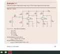
I found a schematic for a cascaded CE and CC amplifier in Malvino's text. After
doing a sim with this circuit I found that the output voltage was 1.04 Volts peak
as opposed to 1.26 volts peak-to-peak in the text. I feel that I have replicated
his circuit and I don't understand the difference in output voltage.

I have included the relevant text (Image 1 and Image 2) as well as the sim file.
 

Attachments

ericgibbs

Joined Jan 29, 2010
18,767
hi 2019,
Your sim circuit is not the same configuration as the Book example, why would you expect to get the same result.?
What is your design requirement, ie: bandwidth etc...

E
 

Jony130

Joined Feb 17, 2009
5,487
You've got different results in simulation because the gain of this amplifier is very strongly dependent on re = Vt/Ic.

In your simulation, you have T = 27°C and Ic ≈ 1mA hence re ≈ 25.87Ω


So the gains are Av1 = 783Ω/25.87Ω ≈ 30.2V/V and Av2 = 2.65kΩ/25.87Ω = 102.4V/V


Therefore the total gain is around 3000V/V instead of 4000V/V.

Or we can look at the situation this way.
Because your Ic current is 10% smaller the gain of each stage will also be 10% smaller. Therefore the overall gain will drop by 20%.
 
Last edited:

Thread Starter

newbie2019

Joined Apr 5, 2019
95
You've got different results in simulation because the gain of this amplifier is very strongly dependent on re = Vt/Ic.

In your simulation, you have T = 27°C and Ic ≈ 1mA hence re ≈ 25.87Ω


So the gains are Av1 = 783Ω/25.87Ω ≈ 30.2V/V and Av2 = 2.65kΩ/25.87Ω = 102.4V/V


Therefore the total gain is around 3000V/V instead of 4000V/V.

Or we can look at the situation this way.
Because your Ic current is 10% smaller the gain of each stage will also be 10% smaller. Therefore the overall gain will drop by 20%.
Thanks. This is the transistor model. Can you tell me how you were able to tell me the temperature etc. from this data?

.model 2N3904 NPN(IS=1E-14 VAF=100 Bf=300 IKF=0.4 XTB=1.5 BR=4 CJC=4E-12 CJE=8E-12 RB=20 RC=0.1 RE=0.1 TR=250E-9 TF=350E-12 ITF=1 VTF=2 XTF=3 Vceo=40 Icrating=200m mfg=NXP)
 

Audioguru

Joined Dec 20, 2007
11,248
The simple circuit has no negative feedback causing the output of the first transistor to have distortion bad enough to make level measurements difficult or impossible. The top half of the waveform is squashed as the transistor approaches being cutoff.
 
Top