Op-amp buffer circuit

Thread Starter

harikrishna125

Joined Sep 7, 2017
13
Hi all,

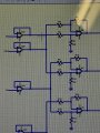
I am working an Op-amp circuit where the op-amp drives the mosfets (N and P-ch), and the output is taken from the source of the two mosfets. please check the picture for better understanding.
similarly I have an other circuit which does the same, the 2 outputs of two circuits is connected to to some external device in such a way that the first circuit if it has 1Volt output then the secound circuit should compensate with 6 volts and vice-versa. The first circit can go upto max 7 volts and the second also max 7volts, making the complete circuit work within +-7 volts.

which OPV is best for RAIL to RAil input /output operation?
 

Attachments

Thread Starter

harikrishna125

Joined Sep 7, 2017
13

ericgibbs

Joined Jan 29, 2010
18,766
Thanks for the reply, the one which you sent is only rail to rail output but I want something which is both input and output in such a way that the inverting adn non inverting outputs should be same within a error of +-1mv
hi,
I am not sure I follow you, are you asking for a R2R that has <=1mV offset between the INV and NI inputs.
You got my point about the LT6023 not being suitable for the circuit in your first post.?

E
 

Thread Starter

harikrishna125

Joined Sep 7, 2017
13
hi,
I am not sure I follow you, are you asking for a R2R that has <=1mV offset between the INV and NI inputs.
You got my point about the LT6023 not being suitable for the circuit in your first post.?

E
presently, I am using RH1498M which has rail to rail of +-14.5 V, I think this works my application, but the question is how to get rid of the switching transients of the mosfet when the load is capacitive at the end and also methods to compensate the parasatic capacitance. ?
 

Thread Starter

harikrishna125

Joined Sep 7, 2017
13
Oh thats really nice. Thanks a lot for the circuit. Can we use the same circuit twice so that the outputs of 2 circuits are connected to a capacitive load of max 200nF ans still the system doesn't show any oscillations.

Because if I use the this circuit then the output is good, but if use 2 circuits in parllel powering a capacitive load then the IN and NonIN inputs of both circuits are swinging because of the switching transients from the mosfets. Is there any other way to get over this problem?
 

Bordodynov

Joined May 20, 2015
3,177
Oh thats really nice. Thanks a lot for the circuit. Can we use the same circuit twice so that the outputs of 2 circuits are connected to a capacitive load of max 200nF ans still the system doesn't show any oscillations.

Because if I use the this circuit then the output is good, but if use 2 circuits in parllel powering a capacitive load then the IN and NonIN inputs of both circuits are swinging because of the switching transients from the mosfets. Is there any other way to get over this problem?
I don't understand how you want to turn on two circuits. I have calculated the bridge circuitry.
2019-07-26_16-15-39.png
 

Thread Starter

harikrishna125

Joined Sep 7, 2017
13
I don't understand how you want to turn on two circuits. I have calculated the bridge circuitry.
View attachment 182485
the circuit works fine, but the mosfets gates are driven from Op-Amp output, not the vcc supply and also the source of N and P-channel are connected instead drain to drain. something like the following picture. The inverting and non inverting of the first op-amp and second op-amp swings like the second picture.
 

Attachments

Last edited:

Bordodynov

Joined May 20, 2015
3,177
the circuit works fine, but the mosfets gates are driven from Op-Amp output, not the vcc supply and also the source of N and P-channel are connected instead drain to drain. something like the following picture. The inverting and non inverting of the first op-amp and second op-amp swings like the second picture.
I wasn't trying to fix your disgusting scheme. I offered mine. Didn't you see from the results of your simulation that you were not doing well. If your goal is to make your scheme work well, I'm sorry, I thought you needed a really working scheme (at least in a simulator).
 

Thread Starter

harikrishna125

Joined Sep 7, 2017
13
You're right. Getting old. And I am irritated by people who ask for help and can't explain what they want.
I am sorry for the late reply, I am actually making a circuit to get an output of +-7 volts at the end. For example is I have an output voltage of +3V at the output the second Op-amp should output 4V so that the total PD is 7V.
if the first opamp has 0V the second one should give -7V so that the PD is 7V.
When I make the circuit in such a way that I uploaded above there is a small time at which both N and P-Mos are switched on and there is short circuit at that point.

I should add a delay between the N and P-Mos switching in such a way that the P-mos will only turn on after N-mos is completely turned off and vice versa so that the transient switching cannot be seen at the output and the signal is neat and clean.

If u still don't understand the complete concept, please let me know.
Thank you.
 
Top