Facebook
 Google
 GitHub
 Linkedin
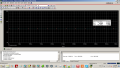
This looks promissing. The first output pulse is sufficiently long to suppress the one at 700µS as requested. But at the following trigger at 1mS gives a short output pulse. What is the cause. C not completely discharged? Is there a solution?D1 is backwards.
Attachments
-
2.7 KB Views: 4