Facebook
 Google
 GitHub
 Linkedin


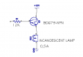
The literature I got from internet says that, if a NPN transistor is to be used as a switch, the load shall be at the power feed side of the transistor and the emitter shall be connected to GND. But, I prefer that, the load will be at ground side of the transistor. My try worked well on the bread board. Please, see the attached drawing for more clarification.
The drawing shows the load as a lamp. But in my project, the load is other electronic circuit with different function, so that my switching circuit with NPN transistor will power on or off the other circuit. Will it be reliable for long term, or damage the other circuit or itself.
Thanks in advance.
The drawing shows the load as a lamp. But in my project, the load is other electronic circuit with different function, so that my switching circuit with NPN transistor will power on or off the other circuit. Will it be reliable for long term, or damage the other circuit or itself.
Thanks in advance.
Attachments
-
 7.6 KB Views: 115