Facebook
 Google
 GitHub
 Linkedin
Hi all,
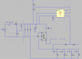
Before I start, I am not an electronics engineer, at best a hobbyist who is working on an Arduino project and is looking to add some protection to the circuit when designing a PCB to put all the bits on. There should be an attachment of the schematic. I apologize if this is a stupid question.
I've been doing a lot of reading and perhaps unnecessarily want to add reverse voltage and over voltage protection the my circuit. The two circuit designs that I had come across were the P-Channel Mosfet for the reverse voltage, and the Crowbar for the over voltage. Now below is my first schematic. It doesn't have all the values for each component at this stage. What I am interested in knowing is if the design would actually work?
From what I understand the M1 PMOS (P Channel Mosfet) will only activate when it has the correct polarity. The Zener D1 will clamp the voltage to 15V. The resistor R1 is there to limit the current that will flow through the zener D1? If the polarity is reversed the circuit will never be complete so no current flows. Am I correct so far?
Next... if the polarity is correct, M1 PMOS allows current to flow. Capacitors C1, C4, C5 I have as bypass caps as the voltage supply will be coming via a rotating slip ring so there could be moments where a good contact is not available so these caps fill in the gaps.
Next I found the LTC1696 which is an over voltage device that monitors 2 voltages. So my theory is when voltage flows, D2 clamps the voltage to 15V, R6 limits the current through D2 (actually I'm thinking I dont need D1 if I have D2?).
The LTC1696 has a threshold voltage of 0.88V on the FB1 and FB2 pins. If more voltage than 0.88 is received on those pins it fires the Out pin. Voltage dividers (R4-R5, R2-R3) are used to set the actual voltage value that you want to trip FB1/FB2.
If FB2 goes over its threshold it fires the Out pin which latches Q1 transister which latches U1 SCR to ground which takes all the current and blows the fuse. This is protecting against the actual supply voltage being to high.
Assuming none of that is triggered, voltage flows to the v7805-2000R non isolated switching regulators. If FB1 goes over its threshold it fires the Out pin which latches Q1 transister which latches U1 SCR to ground which takes all the current and blows the fuse.
I would need to figure out the values of resistors based on what voltage value I am protecting against (say protect up to 50V on the supply, and protect against 5.5V or higher on the switching regulator out side).
Excuse my ignorance, but am I on the right track with this design?
") ), the LTC1696 27V. So if I understand this correctly, the zener D1 and D2 have a power rating, say 1/2 watt and the resistor R1/R6 again we'll say 1/2 watt. So I would have to calculate the R1/R6 resistor value based on 50V so that would be 35V left for the resister to handle. So I=V / R, I = 35V x 5000Ω, I = 0.007 or 7mA. Then P = I x V, P = 0.007A x 35V, P = 0.245 watts. So I could use a 5K resistor to handle the 35V. Am I right so far?
), the LTC1696 27V. So if I understand this correctly, the zener D1 and D2 have a power rating, say 1/2 watt and the resistor R1/R6 again we'll say 1/2 watt. So I would have to calculate the R1/R6 resistor value based on 50V so that would be 35V left for the resister to handle. So I=V / R, I = 35V x 5000Ω, I = 0.007 or 7mA. Then P = I x V, P = 0.007A x 35V, P = 0.245 watts. So I could use a 5K resistor to handle the 35V. Am I right so far?