Facebook
 Google
 GitHub
 Linkedin
I need to design a threestage MOS amplifier that adheres to the following:
1) 1st stage should be a differential amplifier
2) 2nd stage should be common-emitter or common-source
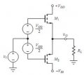
3) 3rd stage Class AB
These specifications need to be observed:
Signal path = DC coupled, no series capacitors
Maximum transistor channel length = 12μm
Output load resistor = 100Ω
Max number of independent sources for bias = 1
Power supply voltage = ±15V
Minimum output voltage at 1KHz = ±12 Vp-p across 100Ω load
minimum single-ended open-loop gain = 50 dB (20logAv0
Max offset voltage for 0V differential input = 20mV for ±15 V supplies
minimum gain-bandwidth product = 10 MHz with 45° phase margin
Max THD at 1kHz = 1% for ±12 Vp-p across 100Ω resistor
minimum CMRR at 1KHz = 70 dB
Max DC power consumption, load resistor = ∞, = 0.75W
If some one could walk me through the stages and help me understand this design process, I would definitely appreciate it very much.
1) 1st stage should be a differential amplifier
2) 2nd stage should be common-emitter or common-source
3) 3rd stage Class AB
These specifications need to be observed:
Signal path = DC coupled, no series capacitors
Maximum transistor channel length = 12μm
Output load resistor = 100Ω
Max number of independent sources for bias = 1
Power supply voltage = ±15V
Minimum output voltage at 1KHz = ±12 Vp-p across 100Ω load
minimum single-ended open-loop gain = 50 dB (20logAv0
Max offset voltage for 0V differential input = 20mV for ±15 V supplies
minimum gain-bandwidth product = 10 MHz with 45° phase margin
Max THD at 1kHz = 1% for ±12 Vp-p across 100Ω resistor
minimum CMRR at 1KHz = 70 dB
Max DC power consumption, load resistor = ∞, = 0.75W
If some one could walk me through the stages and help me understand this design process, I would definitely appreciate it very much.